Your cart is currently empty!
Author: James
How to measure an amplifier using a DSA-815-TG?
How to measure an RF Amplifier using a DSA800 Series Spectrum Analyser
Solution: This document provides step-by-step instructions on using the Rigol DSA800 series of Spectrum Analysers to measure the characteristics of an RF Amplifier.
In addition to the DSA-800 Spectrum Analyser, you will need an RF Source, cabling, and adapters.
Measure the amplifier
1. Connect the RF generator output to the RF input of the instrument using the appropriate cabling and connectors.
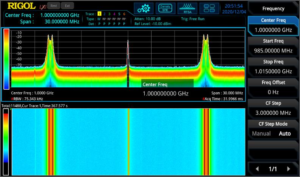
NOTE: If your instrument is equipped with a Preamplifier, you can enable it to lower the displayed noise floor by pressing the following sequence:
Press AMP button > Down Arrow > RF Preamp On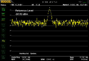
Figure 1: Preamplifier off 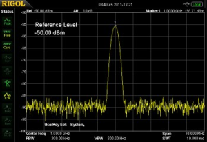
Figure 2: Preamplifier on 2. You can use the Auto button to center and zoom on the waveform. You can also use the Freq and Span buttons to manually manipulate the displayed data.
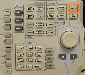
• Another option to center the waveform is to press Freq button > Peak → CF. This will automatically align the center of the display with the peak of the trace.
3. Freeze the unamplified trace by pressing Trace > Trace Type > Freeze. You can use the Marker button to create a marker. This can be used to find the peak frequency and amplitude of the displayed waveform.
4. Disable the RF Generator output.
5. Disconnect RF generator from the instrument RF Input and connect it to the Amplifier input.
6. Connect the Amplifier output to the instrument RF Input.
7. Enable the RF generator.8. Enable a second trace to visualise the amplified signal by pressing the Trace button > Select Trace 2.
9. Set the trace type to Clear/Write by pressing Trace > Type > Clear/Write.
10.You can use the Auto button or manually center the trace using the Freq, Span, and Amp buttons.
11.Readjust the amplitude scale by pressing Amp > Auto
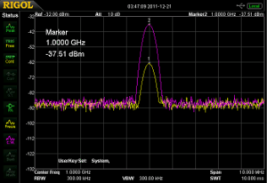
12.You can enable an additional marker for the new trace by pressing Marker > Select the marker you would like to use
13. Now, select the trace you want to mark by pressing Marker > Marker Trace > select trace of interest
• Be sure Normal is selected to enable the marker14.You can also enable a marker table by pressing Marker > Down Arrow > Mkr Table ON. This allows a convenient way to compare markers and values between traces.
15. Alternately, you can use the Trace Math function to create a Trace difference on the screen.
16. Enable Trace Math by pressing Trace > Trace Math
17. Set Function to A-B
18. Set A = T1
19. Set B = T2
20. Set Operate > On21.Set Amplitude by pressing AMPL > Auto
NOTE: New trace appears. This represents Trace 1 – Trace 2.
22. Set Marker to Math Trace by pressing Marker > select Marker 3
23.Set Marker Trace to Math by pressing Marker > Marker Trace > Math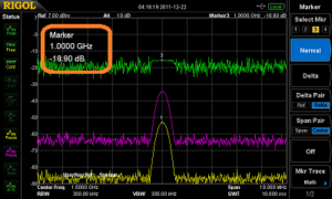
• You can then move the marker to the smoothest portion of Trace 3.
Products Mentioned In This Article:
- DSA800 Series please see HERE
Keyless Entry System ASK/FSK Analysis
RIGOL Technologies extended the RF test system of DSA800 spectrum analyser with additional tests for passive key less entry systems. RIGOL’s test solution is very comfortable to use and much cheaper than other available test systems on the market.
Passive keyless entry [PKE] communication is an electronic lock system mainly used to open cars or buildings without a mechanical key. This lock system works with a passive component (key) which will be activated by a device (e.g. a car) sending a periodical signal to its environment. One most common example is the keyless entry system in a car. The car sends always a constant low frequency [LF] signal around 130 kHz to its environment. If the correct key is closed to the car (~1.5 to 5 meter) then the key recognizes the LF signal and sends back the correct ID with an ASK or FSK modulated RF signal (UHF1). With opening the car door it will be unlocked. With some keys it is also possible to start the car via a button when the key is internally the drivers cab or to open the door of rear trunk. The used frequency of UHF signal depends of location. Mainly ISM2 bandwidth for carrier frequency of 433 MHz will be used in Europe. This application uses also a carrier frequency of 868 MHz in Europe but this frequency range is not part of an ISM bandwidth. USA and Japan use mainly the frequency band of 315 MHz.
Two kinds of procedures are possible3:
1.) Car sends a LF signal with a short wake up signal1 UHF = Ultra High Frequency (range: 300 MHz to 1000 MHz)
2 ISM = Industrial Scientific and Medical Band are bandwidth which can be used with a defined maximum power in industry, scientific, medical or private applications. ISM defines two types: Type A and Type B. Type B bandwidth can be used without requesting an official license. The most popular ISM band is 2.4 GHz to 2.5 GHz, used for WIFI.
Systems in Modern Cars, Aur´elien Francillon, Boris Danev, Srdjan Capkun Department of Computer Science ETH Zurich 8092 Zurich, Switzerland, §2.2- In a defined period a car sends a LF signal with short information to its environment (wake up signal).
- If a keyless entry key is closed to the car, the key sends an acknowledgement (UHF) to the car.
- The key and the car starting a data communication with ID check.
- Car sends an ID to the key. If the ID is correct, the key sends the correct key code. If this key code is correct, then car let you open the door.
2.) Car sends a LF signal with car ID - In a defined period the car sends a LF signal with the car ID to its environment.
- If a keyless entry key is closed to the car and ID is correct, the key sends the correct key code. If this key code is correct, the car can be opened.
FSK – Frequency Shift Keying
Frequency Shift Keying (FSK) is a digital modulation form. The principle of shift keying is to modulate a digital signal to a carrier and the changes are discrete in nature. The basis form is 2FSK. 2FSK is used e.g. in keyless entry systems like a car key or a tire pressure monitoring system. In simplest form of 2FSK modulation two digital state “0” and “1” (2FSK with 1 bit/symbol) will be transmitted with two different frequencies. These two frequencies are modulated to a carrier frequency and both have the same distance to the carrier. The difference to analogue frequency modulation (FM) is that the two transmitted frequency changes in the rhythm of binary data. In FM the frequency changes according to the analogue modulation frequency.
The distance of both frequencies to carrier is defined as FSK deviation: - FSK deviation = Δf
- fcarrier ± Δf
Example:
2FSK with Δf = 40 kHz and fcarrier = 866 MHz is visible in figure 1
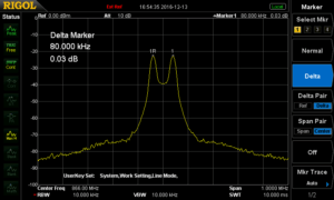
Figure 1: 2FSK Signal with FSK deviation of 40 kHz, fcarrier = 866 MHz, tested with DSA832E The frequency shift of both frequencies is 80 kHz:
- fmax = fcarrier +Δf = 866 MHz + 40kHz
- fmin = fcarrier – Δf = 866 MHz – 40kHz
- fmax – fmin = 80kHz
Frequency shift is 2 x FSK deviation: - Δ(f2-f1) = 2 x Δf
In constellation diagram of a 2FSK signal is visible in figure 2.
The tests performed in figure 3 and figure 4 show different kind of important measurement: - Signal shall not be higher than customer defined pass / fail curve (see figure 3). Test can be performed with a DSA832, DSA832E or DSA875.
- Absolute power values of these two frequencies can be analysed (figure 4, marker 2R and 3D)
- Information of carrier offset can be checked with marker function (figure 4, marker 1D)
- Difference of power values of two frequencies can be measured (figure 4, marker 2R and 2D)
Another measurement is the analysis of occupied bandwidth (OCP). OCP measures the frequency range which contains 99% of spectral power of signal. The carrier frequency is centered in the middle of this frequency range (see figure 5). OCP can be measured with DSA800 with the option DSA800-AMK.
Calculation of OCP for 2FSK is defined as follow: - OCPBW6 = Data rate + 2 x Δf
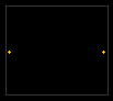
Figure 2: Constellation diagram of 2 FSK, carrier frequency is in the middle 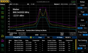
Figure 3: pass / fail mask for curve analysis 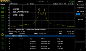
Figure 4: Measurement values of 2FSK signal (see marker table) 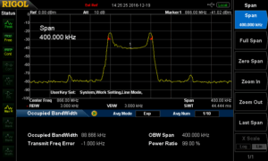
Figure 5: Measurement of occupied bandwidth with a 2FSK signal 4 Speed of DSA832, DSA832E and DSA875 (sweep time of 10 msec: processing time is 30-40 msec.): measure speed of ~50 msec. is possible in normal mode.
5 Following tests can be performed with the option DSA800-AMK: Time Power, Adjacent Channel Power, Channel Power, Occupied Bandwidth, Emission Bandwidth, Signal to Noise Ratio, Harmonic Distortion, Third Order Intercept Point
6 With influence of a roll off factor e.g. with 0.35, OCP will be lower than the calculation.Example: Data rate: 10kSymbols/sec. and frequency deviation: 40 kHz
- OCPBW = 10 kSymbols/sec. + 2 x 40kHz = 90 kHz
Filtering:
The target of filtering is, that the digital pulses will get a smoother rounded pulse form (according a gauss clock) to get better spectral results and reduce the bandwidth. In RIGOL’s software ULTRA IQ STATION it is possible to select different filter types. A special Gauss Filter for FSK modulation is available to reduce the bandwidth before transmission. Filtering of FSK modulation with that kind of filter results this modulation form into a GFSK modulation. In this software it is possible to adjust the roll off factor (α = B*T), the impulse length (amount of samples per pulse with duration of one bit) and oversampling (additional sampling to be better compliant of sampling theorem to use a simpler reconstruction filter). A gauss characteristic is visible in figure 6. The length of filter is the product of Impulse length and oversampling values. Roll-off factor α is calculated with: - the bandwidth (@-3 dB) of gauss characteristic: B
- the duration of one bit: TBit
2FSK Signal can be generated with Software ULTRA IQ STATION and can be downloaded to an RF signal generator with IQ option (DSG3030-IQ or DSG3060-IQ7).
The clock frequency in the generator will set the wavetable output clock rate. This clock frequency will be calculated from oversampling value and symbol rate (One symbol contains one bit in this 2FSK modulation example).
Clock frequency = oversampling value * symbol rate
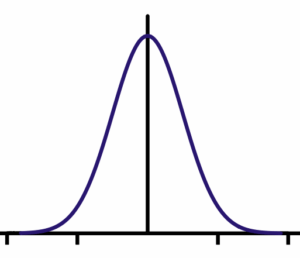
Figure 6: Gauss characteristic Software S1220 for 2FSK demodulation
DSG3030-IQ: 9 kHz to 3 GHz; DSG3060-IQ: 9 kHz to 6 GHz; IQ Modulator is an Option and contains also external analogue I and Q in-, and outputs
RIGOL provides (option) a demodulation software solution for ASK / FSK demodulation with software S1220. This software works with spectrum analyser DSA832, DSA832E and DSA8758. ASK demodulation will be described at the end of this document.
- This software displays the symbol waveforms of modulation
- Eye diagram can be analysed. This is important to see to analyse jitter effects.
- Specific pattern can be set as reference. Each time the pattern will be transmitted, it will be marked in yellow.
- Carrier Power, Frequency deviation and Carrier frequency offset will be measured.
- Manchester encoding is supported.
- Load and save configuration data
FSK Measurement with DSA815 / DSA705 / DSA710
Software S1220 is usable for
DSA832(E)/DSA875. The measurement speed of
DSA815 / DSA705 and DSA710 is lower than
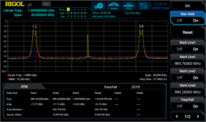
DSA832(E)/DSA875 and their speed for 2FSK signals are too slow. RIGOL solve this problem with a new option for signal seamless capture (SSC-DSA)9. With the option SSC-DSA 2FSK analysis is also possible to do the FSK measurement with DSA815 / DSA705 and DSA710. With this option the analyser switches into a FFT mode with faster capturing speed. FSK signal measurement (up to three different 2FSK signals) can be performed with that option (see figure 10) in parallel up to 1.5 MHz directly with the device without additional software.
This option has three different main features:- Real time trace (RT Trace)
- Maximum hold function
- 2FSK signal capture analysis which includes
8 Analyser will be set into a DMA mode (FFT Mode). The analyser can only be controlled with S1220 in DMA mode. 9 This option is only valid for DSA705, DSA710 and
DSA815o also a maximum hold function parallel to continuous test
o pass/fail measurement according to limit lines to be set
o activation of two mark lines
o measurement of two frequencies from 2FSK signal, amplitude of both frequencies, frequency deviation and carrier offset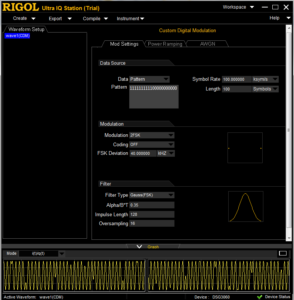
Figure 7: 2FSK Signal generation with ULTRA IQ STATION 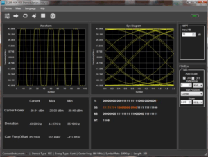
Figure 8: Software S1220 for ASK / FSK demodulation 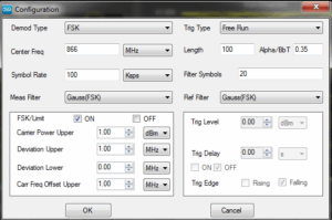
Figure 9: FSK configuration in S1220 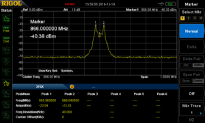
Figure 10: 2FSK measurement with DSA815 and SSC option ASK – Amplitude Shift Keying
ASK is also a digital modulation form used in e.g. keyless entry or radio beacon in navigation. In simplest form, the characters one “1” and “0” of digital signal will be multiplied with a carrier frequency (see figure 12 to figure 14). On/Off Keying is used in keyless entry systems using ASK modulation.
On/Off Keying (OOK):- Carrier will be on with “1”; carrier will be off with “0”.
- ASK modulation is 100% (see figure 14) ASK can also be transmitted with a constant carrier. In this case zero “0” will be transmitted with a lower frequency than one “1”. ASK modulation could be e.g. 10% (e.g. for near field communication [NFC] with a bit rate of 424 kbps).
ASK modulation index will be calculated as follow: - m = (A-B)/(A+B) * 100
- If m = 8-14% then ASK modulation is ~10%.
- Modulation depth is B/A
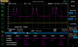
Figure 11: 2FSK measurement with three parallel 2 FSK signals with max hold measurement 
Figure 12: Pulse train with “1” and “0” (digital signal) 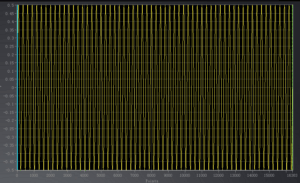
Figure 13: Carrier of ASK (sine signal)) 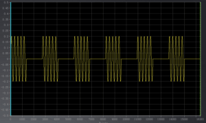
Figure 14: ASK modulation (digital signal * carrier) ASK bandwidth is defined with:
- B = 2 x Symbol Rate
ASK signals can also be generated in RF signal generator DSG3000-IQ (e.g. DSG3060) together with software ULTRA IQ STATION (see figure 16).
The frequency range is visible in figure 17. ASK Spectrum shows the bandwidth of 2 x sample rate. This spectrum is visible with different signal lines. This makes sense because the expectation of spectrum is not only an on/off cw signal of this modulation form. - A pulse in time range is a SI (sinx/x) function in frequency range.
- A (constant 0101..) pulse train in time range is a SI function multiplied with a dirac train (like a train of pulses with very small pulse width) in frequency range.
- The multiplication with a carrier results into a shift of this function to the frequency of carrier.
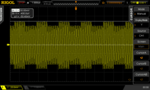
Figure 15: ASK modulation of 10% 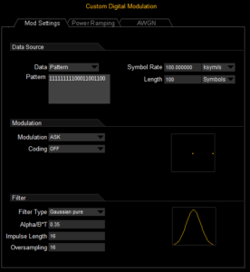
Figure 16: ULTRA IQ STATION settings for ASK generation 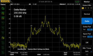
Figure 17: Spectrum of ASK Digital Signal is visible in zero span mode (see figure 18). The pulse train in time range can be analysed in this mode.
ASK signal can also be analysed with RIGOL’s S1220 ASK-FSK demodulation software. Settings and analysis form are the same like for 2FSK analysis.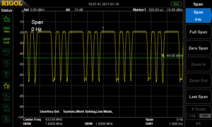
Figure 18: Zero Span analysis of ASK Signal 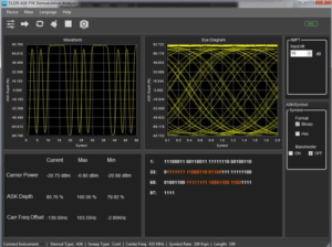
Figure 19: S1220 Products Mentioned In This Article:
EMC Precompliance Testing
Why is Pre-Compliance Testing done?
Almost any electronic design slated for commercial use is subject to EMC (Electromagnetic Compatibility) testing. Any company intending to sell these products into a country must ensure that the product is tested versus specifications set forth by the regulatory body of that country. In the USA, the FCC specifies rules on EMC testing. CISPR and IEC test definitions are also commonly used throughout the world.
To be sold legally, a sample of the electronic product must pass a series of tests. In many cases, companies can self- certify, but they must have detailed reports of the test conditions and data. Many companies choose to have these tests performed by an accredited compliance company. This full compliance testing can be expensive with many labs charging thousands of dollars for a single day of testing. Testing a product for full compliance can also require specialized testing environments. Any failures in compliance testing require that the design heads back to Engineering for analysis and possible redesign. This can cause delays in product release and an obvious increase in design costs.
One of the best methods to lower the additional costs associated with EMC compliance is to perform EMC testing throughout the design process well before sending the product off for full compliance testing. This pre-compliance testing can be cost effective and can be tailored to closely match the conditions used for compliance testing. Pre- compliance Testing can range from basic signal visualization with a spectrum analyser to validation testing against limits or standards and even to interactive debugging. These types of pre-compliance testing require different probes, setups, and tools. Basic visualization, comparison versus standard limits or previous results, and debugging all play important roles in EMI testing to improve your designs, lowers your test costs, and speed your time to market. In this application note, we will compare the advantages, requirements, and available solutions for each type of pre-compliance analysis.
Basic Visualisation
Near Field Probes for Radiated Emissions
The simplest pre-compliance measurements involve visualizing and analysing the magnetic fields resulting from emissions. These test setups start with a spectrum analyser, like the RIGOL RSA3030 (Figure 1). For radiated emissions, use near field magnetic (H field) probes as shown in Figure 2.
Figure 1: Rigol RSA3000 Spectrum Analyser with EMI 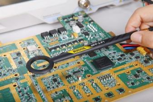
Figure 2: Near Field E and H Probes used to identify EMI Sources Near field probes pick up emissions that pass through the small loop at the end of the probe. These magnetic probes are relatively inexpensive and make it possible to capture signals only in close proximity to the probe, hence the name ‘near field’ probe. This makes them well suited to basic visualization because engineers can quickly scan a new board or enclosure looking for problems by passing the probe over the area as demonstrated in Figure 3. A basic configuration of a near field radiated emissions test would be simply configuring the analyser to use the peak detector and set the RBW and Span for the area of interest per the regulatory requirements for your device. The Peak detector will provide you with a “worst case” reading on the radiated RF and it is the quickest path to determining the problem areas. Then select the proper H field probe for your design and scan over the surface of the design. Larger probes will give you a faster scanning rate, albeit with less spatial resolution.
The probes act as an antenna, picking up radiated emissions from seams, openings, traces, and other elements that could be emitting RF. A thorough scan of all of the circuit elements, connectors, knobs, openings in the case, and seams is crucial. Chambers and shielding are usually not needed for this type of EMI visualization since the probe registers only very close signals. Engineers can often determine the source of an emission by orienting and locating the probe along the test device. The downside to this approach is that there is no easy correlation between near field measurements and compliance results and making repeatable measurements is difficult due to probe positioning. Therefore, engineers must think critically about detected emissions and determine whether they are worth worrying about before going to the expense of further validation.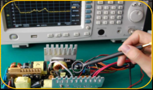
Figure 3: Using an H field probe to test a power supply RF Current Probes for Conducted Emissions
Conducted emissions are unwanted signals that travel via cables. The most common issue is when devices send RF signals back into the power line. There are specific limits associated with these types of emissions designed to protect the power grid and other devices on the circuit. When visualizing conducted emissions engineers use an RF current probe like those in Figure 4. Current flow in a cable placed within the probe is shown on the spectrum analyser. This makes it possible to visualize signals being coupled into a communication or power cable from either the device under test or from external sources. The conducted emissions from a simple LED light fixture are shown in Figure 5. Even simple electronics like this can couple significant power switching frequencies back into the power line. After visualizing these signals care can be taken to filter or improve them if needed before further analysis.
When combined with a spectrum analyser both near field probes and RF current probes are low cost basic visualization solutions for EMI signals. They provide insight without the cost of a more complete EMI system.
Figure 4: RF Current Probes for Conducted Emissions 
Figure 5: Conducted Emission profile of an LED light fixture Pre-Compliance Validation Testing
Limits, Standards, Detectors, and Data Management
Once the testing turns to validation, near field measurements still provide important insights, but the wand style probes can be frustrating since slight changes in position or orientation will affect the results. This makes it impossible to compare to standardized test results or even gauge improvement from one version to another. A full compliance setup with calibrated antennas, an EMI receiver, and a chamber could make final compliance tests, but the cost to setup and maintain this setup can be overwhelming. Fortunately, there are tools that help bridge this gap by making relative analysis simpler. With the right setup engineers can evaluate new designs versus known good designs and compare versus established standards. Getting the most out of this type of pre-compliance validation testing requires additional instrumentation capabilities as well as a more stable test setup.
For this type of pre-compliance testing spectrum analysers should include the standard EMI bandwidths and CISPR detectors. The analyser also needs to be able to segment scans using preferred settings for different areas of the spectrum to optimize sweep time and required accuracy. Most importantly, a spectrum analyser must include standard limit lines as well as the ability to customize limit and margin levels. This is critical because without a calibrated chamber alterations must be made for the test environment in order to build confidence in the results. Lastly, the analyser must be able to create, archive, and compare tests and reports so engineers can problem solve any issues or concerns that arise later in the design process. While not an EMI Receiver, RIGOL’s RSA3000 and RSA5000 series spectrum analysers with the EMI application mode (Figure 6) include all of these features in a single box validation solution.
Figure 6: Rigol RSA5000 Series Real-Time Spectrum Analyser with EMI The EMI measurement mode provides the RSA Series spectrum analysers with limits and CISPR detector modes including Quasi-Peak, CISPR Average, and RMS Average. Engineers also have access to the standard EMI resolution bandwidths (200 Hz, 9 kHz, 120 kHz, and 1 MHz). EMI mode (Figure 7) operates entirely within the instrument from the touch screen or with a mouse and keyboard. This makes it easy to archive reports, run scans, and jump to a signal of interest and immediately debug when needed. The bar graph on the right shows real-time measurements at a given frequency of interest. This utility is made to quickly move to a signal of interest right after a scan without having to change modes. It can show live measurements on up to 3 detectors at the frequency of interest providing an easy transition to debugging and further analysis.
For engineers using a common EMI test software platform, their software toolkits provide flexibility by integrating components from multiple test vendors. Many of these pre- compliance software packages support spectrum analysers including models made by RIGOL. All RIGOL spectrum analysers can be programmed over USB or Ethernet using a standard SCPI instruction set.
EMI Mode on the RSA family of spectrum analysers is a powerful solution providing all the capabilities of a complete EMI validation software package within the instrument.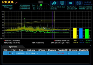
Figure 7: EMI mode using limits, multiple detectors, and meters on a RSA series, Real-Time Spectrum Analyser TEM Cell setups for repeatable measurements
For a test setup with more repeatable measurements than near field probes we can look to TEM Cells. A TEM (Transverse Electro-Magnetic) Cell (Figure 8) is a low cost alternative to measurements in an anechoic chamber. A TEM Cell is a near field device for radiated and immunity measurements. Because the device under test sits at a fixed location within the cell test results are easier to compare and repeat over time than with just a probe. While not directly correlated to far field chamber measurements, a TEM Cell takes repeatable measurements. When used with a complete EMI application tool, new designs can be compared to known good devices and custom limits can be established or developed from known standards that incorporate background emissions, limitations of the test setup, and correction tables. Used in this way, a TEM cell setup with RIGOL’s EMI Mode builds confidence in final compliance results by making it easy to compare good devices, failed devices, and new designs against corrected limit lines with appropriate margin. A repeatable test setup and RIGOL’s EMI Application mode provide an affordable test bed for EMI pre-compliance validation and comparison.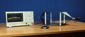
Figure 8: A TEM Cell for repeatable radiated emissions testing EMI Debugging
Real-Time
Once validation tests are completed on a new design, areas of concern are identified and require additional debugging or trouble shooting. Emission issues not captured by basic visualization are often dynamic or dependent on the operating state of the design being tested. These issues can be difficult to capture and understand in a typical swept EMI mode. The combination of a repeatable test setup and a real-time spectrum analyser provide additional debugging capabilities. The RIGOL RSA Series analysers provide multiple views valuable in debugging signals that change over time including density, spectrogram, and power vs time (shown in Figure 9 and Figure 10). In real-time mode the RSA is capable of making seamless measurements. Capture a spectrum without sweeping or missing critical signal activity. Debugging in real-time means that infrequency emissions that might affect compliance are easy to characterize, and with a sense of time, it is much easier to establish the ultimate cause in the design.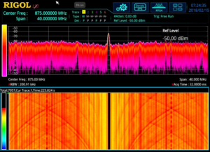
Figure 9: Debugging emissions with the density display (top) and the spectrogram waterfall chart (bottom) 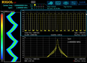
Figure 10: Debugging with a combined view of the spectrum (bottom), power over time (top), and spectogram (left) Debugging with Time Correlation
Additionally, the RSAs have an IF Output. For advanced time correlation of emissions events with embedded signals this IF Output can be input into a mixed signal oscilloscope like the RIGOL MSO7054. This brings the RF signal down to a carrier visible to the scope. In this configuration the RF signal can be viewed alongside digital channels to debug embedded code and communications. To learn more about debugging with the IF output go to our Multi Domain Debugging web page.
Testing emissions with real-time debugging and time correlation for root cause analysis in a repeatable TEM Cell setup is a cost effective system configuration for many of the common EMI design challenges.
Unprecedented Value
EMC Compliance testing is mandatory for the majority of electronic products that are slated for sale throughout the world. Select your instruments and design your test setup to get the most out of your EMI budget for any Pre-Compliance use case. With the right spectrum analyser, visualize emissions with near field and RF probes. Then, validate EMI pre-compliance measurements against known emissions data. Finally, debug and time correlate signals of interest to improve the design. These pre-compliance test setups will help speed product development and save time and money in your design process.Products Mentioned In This Article:
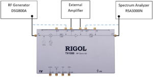
TX1000 Transmitter Education Testing Application Note
Transmitter Functionality – A Perfect Education Training with DSA800 and TX1000 Board
In RF world one of the most interesting techniques is, how to transmit RF data and how does it work? Especially for education market RIGOL Technologies offers a perfect learning tool with spectrum analyser [SA] of DSA800 class1 or using RSA3015N2 [RSA] in combination with a TX1000 demo board. A professor or a teacher will have an easy possibility to demonstrate and show the complex chain of a transmitter or receiver part. A student can follow this lesson and understand transmitter functionality with own hands- on at component level. The overall understanding of RF receivers and transmitters can be learned on a simple way.
This demo board (see figure 1) has the possibility to modulate an RF carrier (500 MHz or 1 GHz) with a base band signal (up to 50 MHz, max bandwidth: +/- 10 MHz). With spectrum analyser DSA815-TG (up to 1.5 GHz) it is possible to stimulate the demo device (via tracking generator) and to analyse it. Alternatively, an external RF Generator with IQ modulation can be used (like RIGOL DSG821A) to test the device with a modulated baseband signal.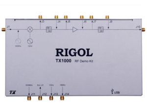
1 DSA815-TG: 9 kHz to 1.5 GHz; DSA832E-TG: 9 kHz to 3.2 GHz; DSA875-TG: 9 kHz to 7.5 GHz. All analysers are available with/without tracking generator.
2 RSA3015N contents sweep based and real time spectrum analyser + vector network analyser and EMI pre- compliance measurement tool with frequency range of 9 kHz to 1.5 GHz (or 3 / 4.5 GHz)The TX1000 demo board incorporates different components:
• 1 GHz local oscillator
• 10 MHz reference
• Mixer
• 1st band pass after mixer
• Amplifier
• 2nd band pass filter after amplifier
Various switches and connection points are integrated on the board. The demo board has the possibility to measure each internal single component or several in different combinations. For example, it is possible to measure the mixed signal after the mixer or to test the amplifier as a stand-alone device. Furthermore, it is possible to omit a component such as a second bandpass filter and use a self- developed one for comparison tests. A block diagram is shown in figure 2.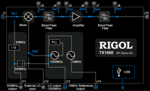
The spectrum analyser series DSA800 provides a built-in control window for the demo board TX1000. All switches can be opened / closed very easily with the spectrum analyser after connecting the demo board to the analyser via USB without the need for an additional PC with software. If only the demo board is the component of interest or the RSA3000N series Real-time Spectrum Analyser (with VNA) is used together with this board, RIGOL also provides free software for this demo board for control via PC.
The first test scenario is the measurement of a signal after each component of the complete chain of the transmission path with the internal 1 GHz fixed local oscillator signal. For the next 4 measurements, an input signal (baseband) is used at port J1. A baseband signal with a frequency range of 50 MHz +/-10 MHz can be used at this port. In the next measurement examples, a constant wave [CW] of 40 MHz and – 10 dBm was used as the baseband input. If the teacher does not have an RF generator available to generate a baseband signal, the tracking generator of the spectrum analyser can also be used as an input (a fast frequency sweep of a DSG3000 can also be used with a start frequency of 30 MHz and a stop frequency of 70 MHz). Each output of the transmission chain can be measured with a DSA800 or RSA3000N series Spectrum Analyzer [SA]. VBW has been reduced in the SA to a lower value than RBW in order to obtain a less noisy trace and also to see small peaks in the test results.
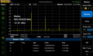
This signal was measured after the mixer process (Figure 1, J3). The measurement in Figure 3 shows the carrier frequency of 1 GHz (marker 1), the wanted signal at 960 MHz (fc – fcw) and the unwanted mirror frequency of 1.04 GHz (fc + fcw). In addition, some unwanted frequency components (920 MHz, 1.08 GHz) are visible. They can all be measured with the spectrum analyser with advanced marker functions.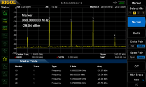
After the first filter (Figure 1, J5), next to the mixer, the mirror frequency is 45 dB lower than in the previous measurement without filter (Figure 4). The carrier at 1 GHz is about 15 dB lower than before. The wanted signal at 960 MHz is also lower by about 3.6 dB because the filter has a max. insertion loss of 4 dB. Both unwanted components are more suppressed than before.
The next additional component after mixer and filter is an amplifier. This component amplifies the main wanted signal with approx. +20 dB. But also the carrier and the unwanted signal components are amplified (Figure 5), as well as the unwanted mirror frequency due to linearity effects of the amplifier.
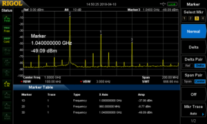
The last component in the transmission chain is a second bandpass filter. This filter suppresses the carrier, the mirror frequency and the unwanted signal components (Figure 6). Most of them are no longer visible at this dynamic setting of the device. The carrier is 65 dB lower than the modulated baseband at 960 MHz.
The next step is to analyse each component as an individual component. The first analysis focuses on the mixer. With the integrated mixer, it is possible to measure the 1 dB compression point, conversion loss and isolation.
For the 1-dB compression point, the same CW sine signal of 40 MHz with a starting power of -10 dBm at the IF input (connector J1) is used. This signal can be generated using RIGOL’s DSG800(A) series or DSG3000B series RF generator. The spectrum analyser is connected to the RF output (J3) of the mixer. The input signal is now increased in 1 dB steps. A linear increase of the mixer signal is expected. If the RF output cannot follow the IF input linearity and deviates by 1 dB, a 1-dB compression point is detected. With the DSA800 or RSA3000N series, different waveforms can be used for this test.
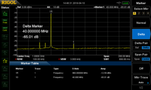
The first yellow trace shows a mixed signal at -28 dBm with an IF input of -10 dBm, resulting in a conversion loss of 18 dB. This trace can be frozen in the spectrum analyser. A second pink trace uses the trace type “clear write”. Now the IF input signal can be increased in 1-dB steps until the mixer output linearity deviates by 1 dB, resulting in a conversion loss of 19 dB. (Figure 7). The 1 dB compression point of the TX1000 mixer is visible at an IF input power of +5 dBm.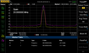
The last tests focused on the entire transmission chain of the TX1000 using a CW signal as intermediate frequency. The next measurements will use a 2FSK baseband signal instead of a CW signal. The focus is on the measurement point after the mixer process to a carrier.
Figure 8 shows an example with a 2FSK signal at the mixer output. The 2FSK baseband is at the IF input with a carrier of 10 MHz, resulting in a distance of 10 MHz from the 1 GHz carrier. This 2FSK figure can be analysed with the real-time mode of the RSA3000N with density/spectrogram. The characteristics of the 2FSK modulation are visible in the lower (wanted) and upper (unwanted) mirror baseband.
The same signal is tested again in the real-time mode of the RSA3000N (Figure 9) using the “Seamless Signal Capturing” function. With this measurement it is possible to measure the frequency deviation and the distance to the carrier of 2FSK signal(s). In addition, the frequency deviation and amplitude level of the 2FSK signal is measured. Furthermore, a pass/fail test of the amplitude tolerances can be performed with this measurement.
Until now, the internal local oscillator of the TX1000 has been used. However, it is also possible to use a self-generated external LO carrier signal using an RF generator such as DSG821(A) (Figure 1, J12) between 50 MHz and 1000 MHz. The oscillator driver power of the TX1000 is +7 dBm, which can be easily adjusted in the DSG800(A).
Figure 10 shows the same signal as in Figure 9, but with external LO carrier of 900 MHz instead of the internal LO. By using the spectrogram in combination with the normal trace, the acquisition speed can be reduced to 100 µsec. It is now possible to measure the details of different data blocks within the spectrogram using delta and Z markers. The difference in frequency, time and amplitude can be analysed in this way.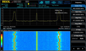
In the next measurement, the focus goes back to the internal LO of the TX1000, where the phase noise can be analysed with the spectrum analyser. The phase noise measurement measures the statistical short-time oscillation around the center frequency. Phase noise can have a significant impact on the quality of the transmitted signal by magnifying spectral lines adjacent to the main carrier that may overlay smaller (wanted) baseband components. Larger baseband components have a worse signal-to- noise ratio. To minimise the negative influence with digitally modulated signals, an LO with low phase noise should be used. The short-term stabilisation of the frequency with an LO depends on the oscillator used. For voltage-controlled oscillators [VCO], a PLL circuit is used to improve their stability.
With the RSA3000N and DSA800 series, it is possible to use a noise marker with the reference to 1 Hz bandwidth. This noise marker can be used to qualify the distance to the carrier [dBc] in amplitude with a frequency offset of, for example, 10 kHz. In the measurement (Figure 11) the typical characteristic of PLL stabilization (two elevations next to the carrier) can be seen on the trace. The measurement of the phase noise of the internal local oscillator of the TX1000 is better than -98 dBc/Hz at 10 kHz frequency offset: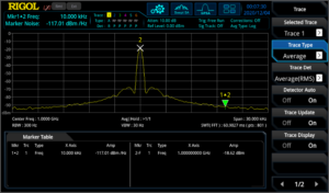
The next part of interest in the TX1000 is the amplifier. Following the same principle as for the mixer (measured in Figure 7), the 1 dB compression point can be analysed to qualify the linear operating range of the amplifier. For the transmission of digitally modulated signals, it is important to have a good and wide linear amplifier range, since digital signals have a high peak-to-average ratio (the amplitude deviation can be very small, but also larger). All these signal components must be amplified in a linear range to avoid negative issues in modulation quality during transmission. With the TX1000 it is possible to disconnect the internal amplifier (J5 / J6 open) and to integrate a self-developed external amplifier into the transmission chain of the TX1000. Comparison tests of different amplifiers can be performed, helping students to design and optimise their own amplifiers (Figure 12).
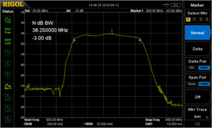
The next measurement will focus on the second bandpass filter. This filter can be measured with the DSA815-TG using the tracking generator at the input. The test cables used can be connected together and normalisation can be performed to avoid their influence on the test result. A 3 dB marker can be used to measure the filter bandwidth at half amplitude of the filter (Figure 13). This S21 characteristic is a scalar measurement, since a spectrum analyser with superposition techniques does not contain phase information.
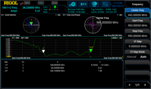
The RSA3000N has a vector network analyser mode. With this mode, S11, S21 or Distance-to-Fault measurements can be performed, since phase information is available in addition to amplitude information. With these functionalities, additional measurements are possible (such as phase over frequency range or with S11, Smith Chart/Polar Chart and accurate VSWR analysis). With the RSA3000N, the S11 back reflection characteristic was measured with the same filter (Figure 14).
The TX1000 in combination with a spectrum analyser such as the DSA815-TG or the RSA3015N is an ideal tool in educational areas such as universities and technical schools to easily demonstrate the complexity of a transmitter’s functionality. Not only can the analysers be used to create a hands-on lab for students, but due to their extreme flexibility, the instruments can be used for many other engineering applications and further R&D measurements. RIGOL also offers an RX1000 board that can be used with the DSG800(A) series RF generator to perform the measurement procedures in the reverse direction to demonstrate a receiver’s functionality. RIGOL offers one of the best price/performance ratios with outstanding RIGOL quality, which is a result of our more than 20 years of test and measurement experience.
Products Mentioned In This Article:
EMC Precompliance: Conducted Emission Testing
EMC Precompliance Testing: Conducted Emissions
Electromagnetic Interference (EMI) can cause undesirable effects on electronic products. These effects can range from annoying glitches to rendering a product unusable.
In an effort to minimise these issues, countries have established standards and limits to products that are being sold within that market. This Electromagnetic Compatibility (EMC) testing is an integral part of product design and qualification for any electronics intended for sale within those markets.
In almost every case, these specifications contain limits on conducted and emitted radiation testing. Conducted emissions are those that propagate through the power line connecting the instrument (Equipment Under Test, or EUT here). Radiated emissions are those that are emitted into the area surrounding the EUT.
This note will briefly cover some common practices for conducted emission testing early in the design phase and we will cover the radiated emissions in another note.A Word about Precompliance
For full qualification testing, a CISPR 16 qualified EMI Receiver and the proper setup must be used. This generally requires using a certified testing lab and special equipment that can be cost prohibitive for development and design tweaking.
This note covers pre-compliance measurements using a Rigol DSA-815 Spectrum Analyser with the optional EMI Measurement Kit (Part Number DSA800-EMI).
While not fully providing fully compliant measurement data, pre-compliance testing can give you critical visibility into the design limitations of your design. You can find the sources of your EMI and try to limit their contributions before the fully compliant testing even begins.
Perhaps the best methodology is to perform a number of pre-compliance tests on a product using a number of physical configurations. Then, compare that data to the data collected in a fully compliant setup.
Using this “Golden Standard” comparison can give you confidence in your pre-compliance measurements and also give you insight into your testing deficiencies. Many of the differences may be systematic and accounted for by allowing for a bigger error cushion on the limits you are testing against.
Physical measurement setup
The more closely you can match a full compliance setup, the more closely your data will match with the lab. But, this isn’t always practical.
The following diagrams show the standard suggested electrical and physical setups for testing conducted emissions: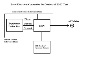
Figure 1: Electrical connections for Conducted EMC Testing. 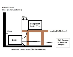
Figure 2: Physical connections for Conducted EMC Testing. The key points:
- The horizontal and vertical ground planes are typically sheets of metal with surface areas twice the dimensions of the Equipment-Under-Test.
- The horizontal and vertical ground planes should be electrically bonded to each other.
- Equipment placed on insulated table over the horizontal ground plane. No equipment or cabling should run below the equipment.
- LISN electrically bonded to the horizontal ground plane. LISN is short for Line Impedance Stabilization Network. Its job is to separate the AC Mains noise from the conducted noise being generated by the Equipment-Under- Test. Please select a LISN that has the proper voltage, current, and frequency ranges for your equipment-under-test.
- Do not coil cables. You want to minimise inductive loops by laying cabling out smoothly.
- The spectrum analyser should be placed some distance away from the horizontal ground plane. Typically, it is a few feet away.
Test Procedure
Once you have setup the EUT and bonded the LISN and ground planes, power on the DSA815 for at least 30 minutes to ensure stability and accuracy.
Configure Spectrum Analyser- Enable the EMI filter by pressing BW/DET > Filter Type > EMI
- Set Resolution Bandwidth by pressing BW > RBW
NOTE: The resolution bandwidth is determined by the standard and specific device type you are testing. As an example, FCC subpart-15 specifies an RBW of 9kHz when testing from 150kHz to 30MHz.
You should consult the standards you are testing to for more information on the specifications governing your testing.
NOTE: Many specifications give limits and values in dBuV or V.
Optional: Set scale for volts by pressing AMPT > Units > VNOTE: The DSA-815 has a pass/fail feature that will allow you to configure an upper limit line. This can be useful when evaluating the frequency scan respect to the limits set forth by the EMC standard you are testing to.
You can also save any limit lines to the internal storage, once it has been created. Simply configure the limit line on the instrument, press Storage > change File Type to Limit, and save the file.
Optional: Add an upper limit line by pressing Trace/ P/F > Pass/Fail > Switch ON > Setup > Upper > Edit and configure point 1 to have an X Axis start at 150kHz with an amplitude of 1mV.
Next, add a point 2 with start at 30MHz and an amplitude of 1mV. Set Connected to Yes for point 2.
This will connect point 1 and 2 with a purple line. This denotes the upper Pass/Fail line.- Set detector type to Peak by pressing BW/Det > Type > Pos Peak
- Set the attenuator to 10dB by pressing AMPT > Input Atten > 10dB
- If the signal is unknown, adding significant external attenuation will minimise the likelihood of damage to the sensitive front end of the spectrum analyser.
NOTE: There are two reasons to add attenuation. The attenuator protects the input circuit from any unknown signals that could damage the input. It also serves as a convenient check on overloading after we check the background readings.
The DSA has protection circuitry, but there are transients that are too fast to protect against.- Set frequency start, stop values set forth in the EMC Specifications that apply to the product. In this example, we are going to configure the instrument to sweep from 150kHz to 30MHz by pressing FREQ > Start and set to 150kHz. Then, press FREQ > Stop and set to 30MHz.
- Set the RBW to the value set forth in the EMC Specifications that apply to the product by pressing BW/Det > RBW > 9kHz
Check background readings
- Power up LISN
- Connect Spectrum Analyser to the LISN output
- Scan over the frequency band of interest using the detector set to Peak and with the attenuator set to 10dB.
- Optional: If you are not using the Pass/Fail line, you can freeze the background trace for reference by pressing Trace/ P/F > Trace Type > Freeze or you can store the trace data by using a USB drive and the storage menu for offline analysis. Either way, noting the peak values and frequencies of the base electrical environment is important.
Peak Test
- Disconnect the Spectrum Analyser from LISN
- Connect EUT
- Reconnect Spectrum Analyser to LISN. This process helps to minimise damage to the Spectrum Analyser due to transients on the input
- On the Spectrum analyser, set up a new trace as Clear by pressing Trace/P/F > Select trace 1 > Trace Type > Clear
NOTE: This setting will overwrite the trace with new data as the scan continues through its frequency range. - Observe the conducted emissions scan.. and adjust the attenuation value to 20dB. If the line does not change for different attenuation values, then it is likely that you are not overloading the input and the measurement quality is high. You can proceed with the pre-compliance testing.
If the scan changes value with different attenuation settings, then it is likely that the input is being overloaded with broadband power and additional attenuation is recommended. You can try comparing scans of 20dB and 30dB, etc.. until a range is found without variation.
You want to select the smallest attenuation value that does not show errors due to the overloading effects of the input signal.
In the worst case, the EUT may not be able to be successfully tested with a Spectrum Analyser. You may need to test using a true EMI receiver with pre-selection filters.Observe conducted emissions and look for frequency lines that are above the limit line you have set. Make note of the frequencies failing the limit lines.
Quasi-peak Scans- Using the failed frequencies above, adjust the spectrum analyser to center the failed peak.
- Note the RBW setting for your scan, and make the frequency span 2x the RBW setting used for the peak scan by pressing FREQ > Start and FREQ > Stop
NOTE: If there is an over limit peak at 10MHz, and an RBW of 120kHz, then you would center your QP Scan at 10MHz, and scan from 9.88MHz to 10.12 MHz. - Change the detector type to Quasi-peak ( )
NOTE: The Quasi-peak detector is based on charge and discharge times of a standardised resonant circuit. This detector type can take greater than 3x the scan time of a peak measurement. That is why it is best to only use Quasi-peak over short spans. The DSA-815 digitally replicates this response. - Compare the quasi-peak data to the pass/fail limit line for that frequency.
- It is advisable to keep the conducted emissions at least 10dB below the
specified limit line. This margin of error will increase the likelihood of passing a full compliance test. - It is also advisable to compare your pre-compliance data and setup to that of the full compliance lab that will perform your EMC certification testing. This will allow you to identify any problems with your pre-compliance testing. With more comparisons, you will be able to hone your pre- compliance error budget and have much more confidence in the results you obtain.
Products Mentioned In This Article:
EMC Precompliance: Near Field Probes
EMC Pre-Compliance Testing: Near Field Probing
Solution: Electronic products can emit unwanted electromagnetic radiation, or electromagnetic interference (EMI). Regulatory agencies, such as the FCC in North America, create standards that define the allowable limits of EMI over specific frequency ranges.
Testing designs and products for compliance to these standards can be difficult and expensive. But, there are tools and techniques that can help to minimize the cost of testing and help to enable designs to pass compliance testing quickly.
One of the most often used techniques for EMI testing is near field probing. In this technique, a spectrum analyser is used to measure electromagnetic radiation from a device-under-test using magnetic (H) field and electric (E) field probes.
In this application note, we are going to describe some common techniques used to identify problem areas using near field probes.
A Word about Pre-Compliance
Most governments have regulations in place that specify the amount of electromagnetic interference (EMI) a product can emit into the environment (radiated emissions) and conduct down the power cord (conducted emissions).
Products being sold within the areas covered by these regulations must comply with the defined test limits. Compliance tests use these regulations to define the proper instrumentation, physical setup, and experimental techniques and experience to correctly record and report properly. This testing is very important and required for legal sale of the product within the covered area. Unfortunately, compliance testing can be expensive and difficult to execute due to the specialised equipment and knowledge required to properly conduct the tests.
Pre-compliance testing simulates the major details of a compliant test setup at a lower investment in time and money. Before you go to a compliance lab for testing, you can use pre-compliance tests to gather information about the performance of a design, make changes (if needed), and retest.. all in an effort to minimize the return trips to the compliance lab.
A word of caution, however. Pre-compliance data can be useful in hunting down many, if not all, of the non-compliant areas of a design but it is not a substitute for testing at a fully accredited compliance lab. Ultimately, the company (you) is responsible for proof of compliance to the full regulations for your product.
Setup
Board level emission testing can be performed using a spectrum analyser, like the Rigol DSA-815 (9kHz to 1.5GHz), near field electric (E) and magnetic (H) probes, and the appropriate connecting cable.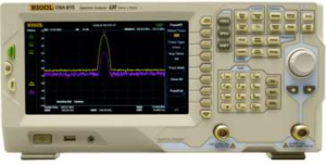
Figure 1: The Rigol DSA815-TG Spectrum Analyser. A commercial example of near field probes are the Rigol NFP-3 probes shown below:
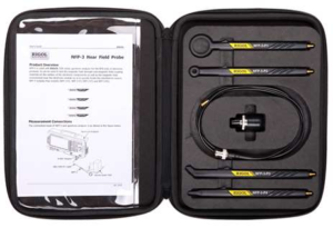
Figure 2: Rigol NFP -3 EMC probes. You can also build your own probes by removing a few cm of outer shield and insulator from a semi-rigid RF cable, bending it into a loop, and dipping in plastic tool dip or other insulating material. Larger diameter loops will pick up smaller signals, but do not have as much spatial resolution as smaller diameter loops.
For the first pass, configure the spectrum analyser to use the peak detector. This setting ensures that the instrument is capturing the “worst case” peak RF. It also provides a fast scan rate to minimize the time spent at one position as you scan over your DUT. Larger probes will give you a faster scanning rate, albeit with less spatial resolution. Smaller probes, like the E Field probe, provide fine spatial resolution and can be used to detect RF on single pins of circuit elements.
Probe orientation (rotation, distance) is also important to consider. The probes act as an antenna, picking up radiated emissions. Exposing the loop to the largest perpendicular field possible will maximize the signal strength. You can also use a fixture to hold both the Device-Under-Test (DUT) and the probe. This will help create repeatable measurements and minimize differences in measurements due to probe orientation.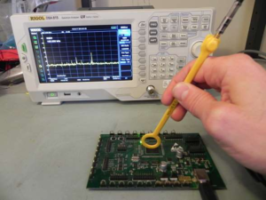
Figure 3: An example of using an H field probe and spectrum analyser to find trouble spots on a board. Note the orientation of the H field probe Take care to test enclosure seams, openings, traces, and other elements that could be emitting RF. A thorough scan of all of the circuit elements, connectors, knobs, openings in the case, and seams is crucial to identifying potential areas where RF can “leak” out of an enclosure.
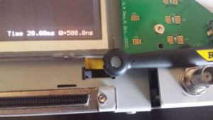
Figure 4: Measuring a display ribbon cable for emissions using an H field probe. You can use tinfoil or conductive tape to cover suspected problem areas like vents, covers, doors, seams, and cables coming through an enclosure. Simply test the area without the foil or tape, then cover the suspected area, and rescan with the probe.
Once you have identified the physical locations of the areas that have the highest emissions, you can get more detail by implementing a few common techniques. If possible, select a spectrum analyser that has the standard configuration used in full compliance testing. This includes a Quasi-Peak detector mode, EMI filter, and Resolution Bandwidth (RBW) settings that match the full test requirements specified for your product.
This type of setup will increase testing time but should be used on the problem areas. A full compliance test utilizes these settings.. and so, your pre-compliance testing with this configuration will provide a greater degree of visibility into the EMI profile of your design.Conclusion
In closing, near field probes and a spectrum analyser can be useful tools in troubleshooting EMI issues.
– With H field probes, try different probe orientations to help isolate problem
areas
– Remember to probe all of the seams around any enclosure surrounding electronic components/boards.. surface contact and finish effect grounding and shielding
– Openings in enclosures radiate just like solid structures. They act like
antennas.
– Ribbon cables and cables/inputs with bad shielding and grounds are common causes of radiated emissionsProducts Mentioned In This Article:
Measuring Cable Loss with a Spectrum Analyser
Testing Cable Loss with a Spectrum Analyser
Solution: A spectrum analyser with a tracking generator can be a useful piece of test gear. This application note covers making a simple loss measurement on a coaxial cable with BNC connectors.
Required:
– Two N-type to BNC Adapters. Select adapters that convert N-type (in/out connectors on most spectrum analysers) to the cable type you are testing. Also note that higher quality connectors (Silver plated, Beryllium Copper pins, etc..) equal better longevity and repeatability.
Figure 1: N-type to BNC adapter – A short reference cable with terminations that match your adapters and cable- under-test.
– An adapter to go between the reference cable and the cable-under-test. This experiment will use a BNC “barrel connector”. Note that higher quality connectors (Silver plated, Berylium Copper pins, etc..) equal better longevity and repeatability.
Figure 2: BNC barrel adapter – Alternately, you can use two adapters a short cable as a reference assembly to normalize the display before making cable measurements. This removes the need to have the cable-to-cable adapter.
– Spectrum analyser with Tracking Generator (TG) Steps:
1) Turn on Spec An and attach adapters to the tracking generator (TG) output and RF Input.
2) Connect the reference cable to the TG out and RF In.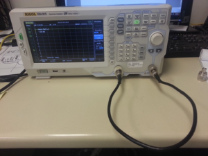
Figure 3: Measuring reference cable 3) Adjust Span of scan for frequency range of interest.
4) Adjust TG output amplitude and spectrum analyser display to view the entire trace.
5) Enable TG.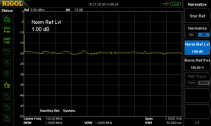
Figure 4: Reference cable insertion loss before normalisation. 6) Normalize the reference insertion loss. This mathematically subtracts a reference signal (stored automatically) from the input signal.
– With the Rigol DSA815 Press TG > NORMALISE > STOR REF and then Enable Normalise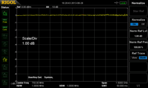
Figure 5: Reference cable insertion loss after normalization. 7) Disconnect the reference cable from the RF input.
8) Place cable-to-cable adapter (BNC barrel or other) and connect to the cable to test.9) Connect the cable-under-test to test to RF input and enable the TG.
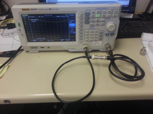
Figure 6: Cable-under-test connected. The screen displays the cable-under-test losses plus the error of the cable-to-cable adapter.
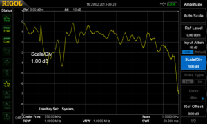
Figure 7: Cable-under-test loss. Products Mentioned In This Article:
- DSA800 Series please see HERE
Using probes with a Spectrum Analyser
Using a Passive Oscilloscope Probe with a Spectrum Analyser
Solution: Spectrum Analysers are typically used to measure radio frequency (RF) signals. The signals are usually delivered to the RF input of the analyser with an antenna, magnetic probe, or using a cable with a matched impedance. This minimises impedance mismatching which lowers reflected power and provides the cleanest measurement. This is not always an acceptable connection scheme. Especially in circuits that are highly susceptible to loading when attached to low impedance inputs, like those on most Spectrum Analysers.
This application note covers using a passive probe, typically used with an oscilloscope, with a spectrum analyser. We highlight some of the advantages and trade-offs with this technique as well.
Most analysers feature a 50 Ohm input impedance. In fact, many oscilloscopes with analogue bandwidths above a few hundred MHz also feature a 50 Ohm impedance setting. This lower impedance enables better performance at higher frequencies but can significantly load a circuit with higher impedance.
In this application note, we will use an RF signal source to deliver a -10dBm signal at 1GHz (CW Sine Wave) to a spectrum analyser, using a passive 1.5GHz oscilloscope probe.Here is a screen capture of the signal directly connected to the input of the spectrum analyser using coaxial cable and BNC adapters:
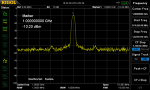
Note that the marker above shows the peak at 1GHz with an amplitude of -10dBm. Now, we connect a 1.5GHz Passive Probe (Rigol RP6150 Passive probe) to the input of the spectrum analyser. The RP6150 is designed to be a 10:1 probe when connected to 50 ohms.
Using a probe with an impedance greater than 50 ohms acts as a voltage divider for signals being delivered to the spectrum analyser. This decreases the voltage to the input and effectively acts as an attenuator. It also has the advantage of lessening the circuit loading that can be caused by connecting the 50 ohm spectrum analyser input directly to the circuit.Here is the same signal but instead of a direct connection to the RF input, we are using an RP6150 probe to detect the signal.
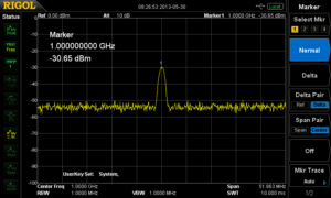
Note that the marker now shows -30dBm for the amplitude. This is due to the probe attenuation factor.
Let’s take a closer look at that probe. Recall that power is the square of the amplitude. Therefore, you can calculate the probe power ratio by simply squaring the probe attenuation factor.Some common probe attenuation ratios can be found using Table 1.
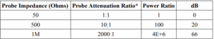
Table 1: Probe Impedance to dB
*With 50 Ohm Input to Spectrum AnalyserNow, we can easily calculate the expected measured power using the equation below: Measured Power (dBm) = Signal Source Power (dBm) – Probe Attenuation ratio (dB)
So, if our Signal Source Power is -10dBm, and the probe attenuation ratio for our RP6150 Passive Probe is 20dB, we would expect to read -30dB on the spectrum analyser as we see in the above screen capture.
For convenience, we can then use the spectrum analysers internal reference setting to adjust for the attenuation of the probe.
Simply press AMPT and set the Ref Level to the probe attenuation ratio in dB. This is a scalar factor that will remove the additional attenuation from the displayed value and give the corrected power value.
Products Mentioned In This Article:
- RP6150 please see HERE
Active loads and the DP800, DP1000 series of Power Supplies
Active loads and the RIGOL DP800 and DP1000 Series 1.
1. Introduction
The RIGOL DP800 series and DP1000 series are programmable linear DC power supplies. They can only provide power for a pure load that does not have the ability to output a current.
Active loads, such as those that can provide power (batteries, solar cells, etc..), should not be used with the DP800 series or DP1000 series power supply. Active loads can lead to instability in the power supply control loop and may damage the powered device.
Connecting the power supply to active loads is not recommended.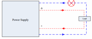
Figure 1 Improper use of DP800 and DP1000 Series Power Supply 2. Detailed Technical Description
The RIGOL DP800 series and DP1000 series programmable linear DC power supply can only work in the first quadrant (source positive voltage and a positive current) or the third quadrant (source negative voltage and a negative current).
They cannot work in the second quadrant (negative voltage, positive current.. an adjustable load of negative power) or the fourth quadrant (positive voltage, negative current.. as used for a battery discharge test).
When the load itself is a source and the power supply is required to work in the second quadrant as an adjustable load, the control loop may lose control and the power supply will output an uncontrolled voltage. This could damage or destroy the load.When the power supply works in the fourth quadrant (e.g., used in a battery discharge test), the control loop is also unstable and will quickly drain the battery. This can result in dangerous conditions, including damage to the battery, power supply, and a very high risk of fire and explosion.
2.1.Power Quadrants in more detail
The Cartesian coordinate system is a common representation of power supply output capabilities. The horizontal axis represents voltage, and the vertical axis represents current. The distributions of the four quadrants of the power supply as shown in Figure 2.
The first quadrant: the power supply provides a positive voltage and a positive current (the direction of the current flows from the power supply to the load).
The second quadrant: the power supply provides a negative voltage and a positive current (the direction of the current flows from the power supply to the load).
The third quadrant: the power supply provides a negative voltage and negative current (the direction of the current flows from the load to the power supply).
The fourth quadrant: the power supply provides a positive voltage and a negative current (the direction of the current flows from the load to the power supply).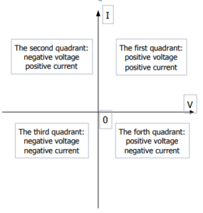
Figure 2 Distributions of Power Quadrants 2.2.Principle of DP800 and DP1000
Here is a block diagram of DP800 and DP1000 series: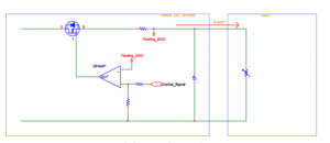
Figure 3 Block Diagram of DP800 and DP1000 If a current is forced into the supply (I.E. sinking the current), it will directly affect the working status of the MOS transistor and result in instability within the control loop of the power supply as shown in Figure 4.
Figure 4 Current Anti-irrigation Diagram In addition, the DP800 and DP1000 series power supply outputs do not have an output relay. When a specific output channel is disabled (power off) the output voltage is set to 0V and is regulated by the control loop.
For charging batteries with the DP800 and DP1000 series power supplies, we recommend using constant current mode and implement the circuit shown in Figure 5. The external diode can prevent the flow of current into the supply and prevent damage.
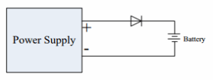
Figure 5 Application Program of Battery Charge Test Products Mentioned In This Article:
- DP800 Series please see HERE
Converting DP800 Record *ROF Files
Reading Rigol DP800 Record (*.ROF) Files with Excel
Solution: The Rigol DP800 series of power supplies have the option to data log the output voltage and current using the Record feature.This application note covers how to convert the binary file format native to the record file type (*ROF) to decimal using HxD (A hex-to-decimal software package) and the ReadDPROF file, a worksheet created using Microsoft Excel 2010.
The end of this document describes the format of the data in the *ROF file and the Excel functions that were used to convert each data point to decimal.
Steps:
1) Configure the DP800 outputs and Devices (DUTs) for your experiment
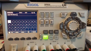
2) Insert a USB stick (FAT32 format) into the USB slot on the back panel of the instrument3) Enable the record feature by pressing the (…) button on the front panel
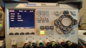
– Set the time per sample to record by pressing Period and use the keypad or wheel to increment the time
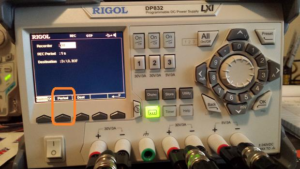
– Select the destination by pressing Det > Select Browser to highlight the external USB (D:) drive
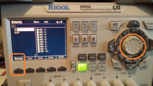
– Press Browser to enter the D: > Press Save and input the file name
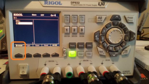
– Press OK when finished entering the filename
4) Enable the Recording by pressing SwitchOff. It will turn to SwitchOn when recording is active.
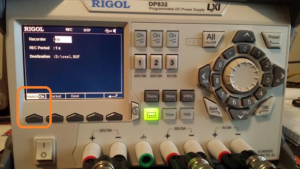
NOTE: The instrument is collecting data as soon as the Recording is enabled.
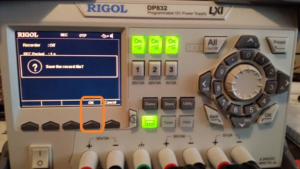
5) Enable the outputs or run the output profile using the Timer function6) Once the test is completed, press (…), and disable the Recorder. As soon as it is disabled, the Record mode will ask if you wish to save the data. Press OK to save.
7) In this experiment, I had the following static output values for the duration of the test:
CH1V = 2.00V CH1A = 0.02A CH2V = 2.08V CH2A = 0.18A CH3V = 1.50V CH3A = 0.33A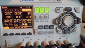
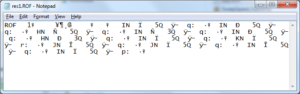
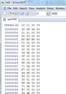
8) Remove the USB stick and insert it into a computer. If you open the *ROF file (res1.ROF is use d in this example) you will see the binary values:
9) Open the ROF file using hex to decimal conversion software. In this example, I am using HxD, as shareware program from http://mh- exus.de/en/hxd/
10) Here is the data in HxD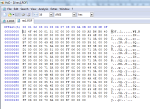
11) Configure HxD bytes-per-row to 4:
Before: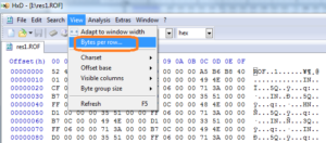
After:
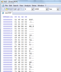
12) Set Visible Columns to Text
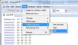
13) Now the data should show the Offset and Hex Values
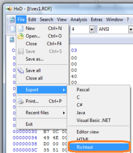
14) Click Export and select
15) Now, open the ReadDPROF.xlsx workbook and select the RawDataFile Tab (at the bottom):
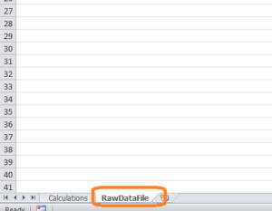
16) Select Data: Import Text, set file type to ALL, select the *RTF file (this is the rich text conversion file from the HxD program)
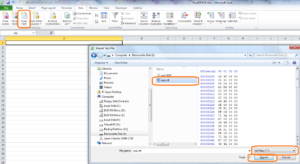
17) Select Delimited and Next
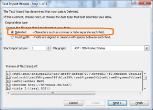
18) Deselect Tab, select Space , and Finish
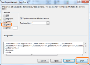
19) Select Cell A1 for import and press OK
20) Now, the formatted data will be transferred to the Excel Sheet
21) Click on the Calculations tab to see the reformatted data
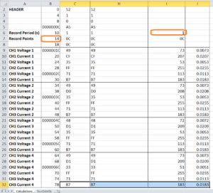
The raw data format (*ROF) returns the record period, number of record steps, the Voltage, and Current of all channels.
The calculations tab of the Excel sheet is designed for use with the three channel DP800s and is only formatted for the first four data points. You can the final row of cells to cover all of the data points for your application as well as re-label the channels.Each data point in the *ROF file is 4 bytes long. To calculate the actual decimal value, the sheet:
– Reorders the bytes (AA BB CC DD to DD CC BB AA) using the Excel MID function
– Concatenates the bytes using the CONCATENATE Excel function – Converts hex to decimal using the Excel HEX2DEC function
– Divides the decimal conversion by 10,000.Products Mentioned In This Article:
- DP800 Series please see HERE
Temperature Measurement App Note
Every electrical and electronic device brought to market has to be classified and tested based on international guidelines, rules, critical values and safety conditions. Each instrument or device that passes is labelled with a special mark. In most of European countries, this will be declared by CE mark. In the US, there is an FCC approval as well as sometimes a UL listing. This identification has been established to be a standardised quality benchmark of design and manufacture. To get this certification, many tests have to be completed before a product can even be sold. One of the most common is EMC tests including interference testing and electromagnetic compatibility. Additionally, there are commonly power and environmental test requirements. Depending on the device itself, there are additional mechanical tests related to vibration or climate to be done. HALT testing (Highly Accelerated Life Test) combines vibration and temperature profile tests.
HALT is applied to the electrical and electronic components during their design phase. The devices will be stressed to achieve an accelerated aging. This is done to find possible problems that can occur during the lifetime of the product. The device will be stressed beyond the specified maximum specs (electrical and mechanical) in order to predict failure modes and future issues. Problems found based on such stress gives designers an opportunity to make improvements that can impact the long-term quality and vitality of a product before it even comes to market.
With this testing it is possible to detect possible quality issues already during the early design phase. This saves time and money, because the later in the developing phase problems are found the more expensive and time consuming the corresponding design changes. So HALT testing helps to reduce the design time and therefore reduce the time to market and also reduce the cost of the final product, so it is a very important test during the design phase of a product.
To conduct a HALT test, the device is positioned on a vibration table inside of a climate chamber. The test normally would consist of cycling of different steps, for example: cool down then heat up in a temperature change test, vibration test, or a combined stress tests. During all these test steps, the device has to be controlled and monitored with measurements stored permanently for the duration of the complete test time. Done correctly, a HALT test cycle can be an automated series of evaluations.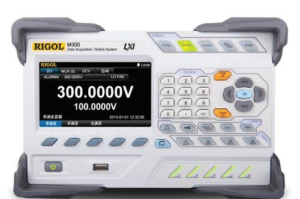
Temperature Measurements
Let’s look at the temperature measurement which is normally done at different locations on or around the device under test (DUT) to get a complete picture of the device’ temperature distribution during the HALT test. To be able to measure such a temperature profile within a climate chamber, you need a robust and accurate array of sensors. In this case a thermocouple is the best solution. A thermocouple is simple and robust with a broad temperature range. They are also cheap and easy to handle. The disadvantage of thermocouples is that you need a reference junction to improve accuracy. The compensation can automatically be done by an instrument like the MC3065 DMM module that is an available module for the M300 test system.Most of the M300 switching cards include a CJC (Cold Junction Compensation) so you can measure the absolute temperature of each thermocouple. This can improve accuracy without an external reference such as ice water for comparison. There are 3 ways to provide a reference source for temperature measurements on the M300 system.
First, select a fixed reference for the highest measurement precision. This is traditionally done by putting the thermocouples in an ice bath to keep the junctions where the thermocouples meet the copper from the measurement system at a constant and known temperature. The ice bath maintains a very precise temperature as it melts to keep the liquid exactly at the melting point. Because this method can be difficult to maintain there are 2 other ways to approximate compensation for the additional junctions.
The most convenient method is to use an internal CJC. The M300 terminal blocks have an isothermal area that includes a temperature reference that can be measured by the DMM. Because the junctions between the measurement system and the thermocouple that we don’t want to measure are on the terminal block we can use the local temperature to predict offset voltage from these junctions and improve accuracy of our measurements. While not as accurate as an ice bath, this is a reliable method for correcting some measurement errors.
Lastly, the M300 system allows users to set one of the channels as an external reference. Implement this method with a more precise RTD or Thermistor that works well in your environmental range. This can provide a more accurate reading of cold junction temperatures than the internal CJC, but will be less accurate than an ice bath because there is more temperature differential across the terminal blocks that create offset.
Also the nonlinearity of the thermocouples is not a big problem because the build in multimeter takes over the calculation from voltage into temperature for all different types of thermocouples (K, J, E, etc.) Each type differs in accuracy and useful range.
Thermocouples utilise the Seebeck Effect. The Seebeck Effect is based on the physical effect that two different metals that are connected together generate a voltage related to the temperature differential of the pair of junctions of the metals. This voltage is very low, for example for a Thermocouple Type K might change 40 uVolts for every 1°C. Therefore you need a voltmeter with high resolution and accuracy like in the M300 6 ½ digit system.
For the complete test it is also necessary to be able to measure more than just the temperature. Other parameters such as voltage, current, resistance can be relevant. It is also very useful to have math functions included in the system because you can define different types of sensors to measure parameters such as pressure, movement, and more.
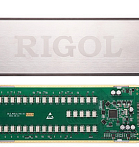
Rigol’s M300 Data Acquisition System
Rigol’s M300 is a complete test solution with build in capability to measure a wide range of physical and electrical parameters. Measurements of up to 256 points are possible per mainframe for temperature, voltage, current, or resistance with a common low connection, or 128 true 2 wire differential signals.
The differential modules can also be configured for automatic 4 wire resistance measurements.
Beside the measurement part, it is also possible to operate
as a control unit. With modules containing analogue and digital outputs as well as external source switching, we are able to react programmatically to process limits in order to shut down, reconfigure, or alert the engineer of a change during the automated test.
• Integrated CJC (cold junction reference) for reference temperature of Thermocouples
• Build in tables of voltage for temperature conversion
• High resolution voltage measurements down to 100nV
• Digital IO cards with up to 64lines
This is just a small selection of the build in functionality of the M300 system
There are many industrial application areas where it is absolute necessary to do these measurements described above as efficiently as possible including:
• Consumer Electronics – even including Washing Machines, Dishwasher, stovetops but also everything from phones and computers to toasters and doorbells.
• Automotive – Validation in temperature chambers of electronic parts.• Aerospace, Transportation, Telecomm – climate/temperature overview for components, critical systems, engines, Base-Stations, etc.
• Power Plants – temperature profile of cooling towers, transformers, relays, and fusesTo make the configuration and measurement much more effective and easy to use, the M300 comes with a PC based data logging Software called UltraAcquire.
UltraAcquirePro is the extended version of the standard software tool and allows use of more than one mainframe in a single test configuration enabling extended graphing capability, data storage, and more.An example of a typical configuration that includes voltage measurements, resistance measurements, frequency measurements and temperature measurements with different sensor types (PT100, Thermocouple Type K, Type E, Type N) can be seen in Figure 1. With the software you can define how each sample is measured, how fast the scan should be and how quick or how accurate each measurement will be and how the data should be stored.
Scans can also be easily configured from the front panel as shown in Figure 2. Monitor up to 4 channels in real time on the front panel during continuous scans (as shown in Figure 3) without connecting the instrument to any software or computer. This is great for industrial or hard to reach signals where local computer control is unavailable or undesirable.
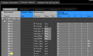
Figure 1: Configuration example using UltraAcquire software 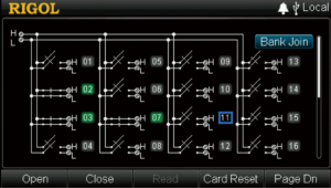
Figure 2: Switch configuration on the M300 display 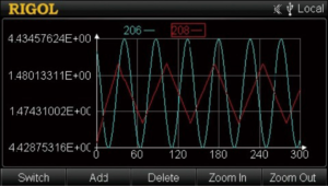
Figure 3: Channel monitoring on the M300 display Products Mentioned In This Article:
M300 System Measurement Primer
Introduction to data acquisition with Rigol’s M300
The M300 Data Acquisition System is designed for automated multichannel measurement and switch applications. This includes environmental measurements like temperature for burn in tests as well as voltage, frequency, or resistance measurements from a wide variety of sensors used from research to production test. These applications are actually very common across a number of industries from electronics to research including a large component of environmental applications.Rigol’s M300 system will cover many of these applications at a considerable price/performance advantage versus traditional solutions. Keys to successful system implementation for your application revolve around proper upfront design and planning. These questions include:
What modules and accessories do I need?How fast will the system go?
What accuracy should I expect on my measurements?
Rigol’s solution provides a production quality alternative at an impressive performance and value. Our large format display and advanced software capabilities allow users from technician level to test engineer get the most out of the system with ease.
Key Applications
CJC Compensated Temperature
Temperature measurements is one of the most common configurations for M300 systems. Large channel count temperature measurements are used in research to industrial settings wherever environmental chambers are used or any kind of lifetime/burn in testing is done. Using 64 channel MUX modules, a single M300 mainframe can scan up to 256 channels (4 64 channel modules and 1 DMM module in a system). For temperature measurements, make sure to get the terminal block accessories since they have the CJC reference that will improve accuracy.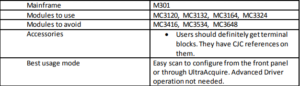
Voltage and 2-Wire Resistance
Voltage and 2-Wire Resistance will usually follow the same configuration as a basic temperature scan. The 64 channel cards only switch the high signals. Some systems may require switched LOs if the signals cannot be all ground or common referenced. For these cases, select the 32 channel MUX module (MC3132) or the 20 channel MC3120.
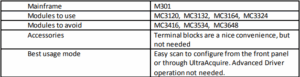
4 Wire Resistance Measurements
4 Wire Resistance Measurements are for higher accuracy and precision. They are more common in scientific and research communities, but can also be used for very sensitive temperature measurements with RTDs. Use either the MC3120, MC3132, or MC3224. The MC3324 adds 4 current measurement channels, but the MC3120 or MC3132 is more cost effective if only 4 wire measurements are required.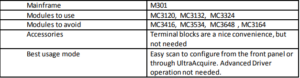
Current Measurements
Large systems of current measurement are not very common, but current measurements are an important part of many test systems. The MC3324 has 4 current channels mixed with 20 voltage channels in a normal configuration. Current measurements are shunted when not connected to the DMM so that the source does not see an open circuit.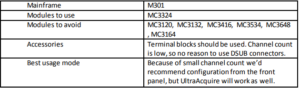
Matrix Applications
Matrix applications are all about signal routing as there are no measurements. The signal in one column can get routed to any row with one switch. It is also possible to connect one column to multiple rows or even to another column if needed using multiple switches. Configuration on these systems is usually tougher because of their general size and the complexity of connecting between cards using the backplane or external jumpering. Accuracy is the key for these systems. Often, the customer will be interested in low voltage offset, high voltage, high current, or even bandwidth. Refer to the module specifications for these – remember the matrix card does not connect to the DMM, so those specifications are not relevant.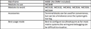
Mixed and Multifunction Applications
These applications require a mix of the capabilities above or some of the more specialised DAC, Totaliser, DIO, or actuator functions. Most applications will not be that varied, but some will be largely multiplexer systems with a few DACs or current measurements mixed in. Simply make sure you have the right number of channels for each capability and consult with applications support to be sure.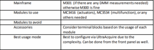
Actuator Systems
These applications usually require higher voltage, current, or power to external systems so they use the Actuator module MC3416 instead of more standard modules. Each card has 16 SPDT channels that do not get connected to the DMM. Each channel is set to connect the COM to the NO or NC position. One of them is always connected to the COM.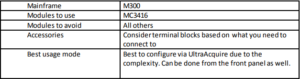
Rigol’s M300 Provides all the necessary tools for configuring your automated acquisition system for performance and accuracy at an unprecedented value.
Products Mentioned In This Article:
- M300 Series please see HERE
- All channel cards are listed as optional accessories on M300 models.