Your cart is currently empty!
Author: James
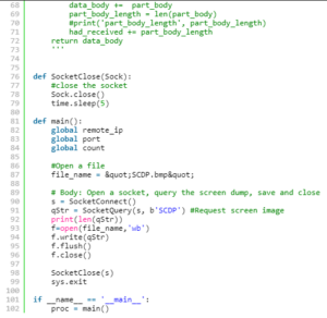
Programming Example: SDS Oscilloscope screen image capture using Python over LAN
Here is a brief code example written in Python 3.4 that uses a socket to pull a display image (screenshot) from a SIGLENT SDS1000X-E scope via LAN
and save it to the local drive of the controlling computer.NOTE: This program saves the picture/display image file in the same directory that the .py file is being run from. It will overwrite any existing file that has the same name.
Download Python 3.4, connect a scope to the LAN using an Ethernet cable, get the scope IP address, and run the attached .PY program to save a bitmap (BMP) image of the oscilloscope display.
Tested with:
Python 3.4
SDS1202X-E
SDS1104/1204X-E
SDS2000X-E Models
SDS5000X Models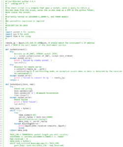
Measuring Power Supply Control Loop Response with Bode Plot II
Introduction
Stability is one of the most important characteristics in power supply design. Traditionally, stability measurements require expensive frequency response analysers (FRA) which are not always available in a laboratory. SIGLENT has released Bode Plot Ⅱ features to the SIGLENT SDS1104X-E, SDS1204X-E, SDS2000X-E, SDS2000X Plus, and SDS5000X series of oscilloscopes. When combined with a Siglent arbitrary waveform generator (SDG or SAG) and an injection transformer, quick frequency response curves can be created.
In this application note, we will show you the basic principles for making this stability measurement and how to use these instruments to make the measurement.
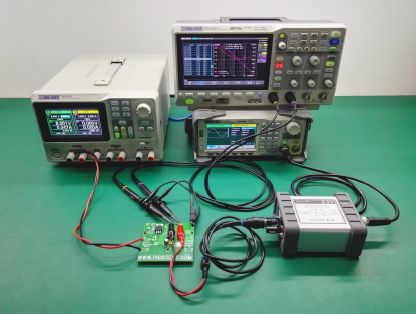 Figure 1: Bode II setup
1. Basic Principle of Stability Measurement
1.1 Stability of The Feedback System
A regulated power supply is actually a feedback amplifier with a large amount of current sourcing capability. Any theory that applies to a basic feedback amplifier also applies to a regulated power supply.
In feedback theory, the stability of a feedback system can be determined by evaluating the loop transfer function. A more practical way is to measure the bode plot of the loop gain. Figure 2 shows a typical feedback system.
The closed-loop transfer A is the mathematical relationship between input x and output y. The loop gain T, by its name, is defined as the gain of a signal traveling around the loop.
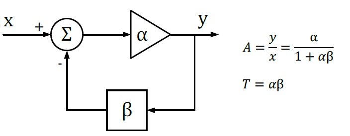 Figure 2: Typical Feedback Loop
Since α and β are complex variables, they have not only magnitude but also phase angle, as also does the loop gain T. If the phase angle of T reaches -180° while the magnitude is 1, the closed-loop transfer function A becomes infinity. In this situation, the system will maintain an output signal while there is no input. Thus, the system acts as an oscillator rather than as an amplifier, which means that the system is not stable.
If we plot the loop gain in a bode plot, we can evaluate the stability by finding the phase margin and gain margin. A phase margin is defined as how many degrees the phase can be decreased before reaching -180°while the magnitude is 1 (or 0 dB). The gain margin is defined as how many dB in magnitude can be added before reaching 1 (or 0 dB) while the phase is -180°.
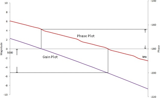 Figure 3: Bode Plot, phase, and gain margin
1.2 Break the Loop
To get the desired loop gain, we simply break the loop. Figure 4 shows how to break the loop in a typical feedback system. Technically you can break the loop any place you like. We commonly choose to break the loop at the point between the amplifier output and the feedback network. Then we insert a test signal i to travel around the loop. The loop gain is the mathematical relationship between the output y and the test signal i.
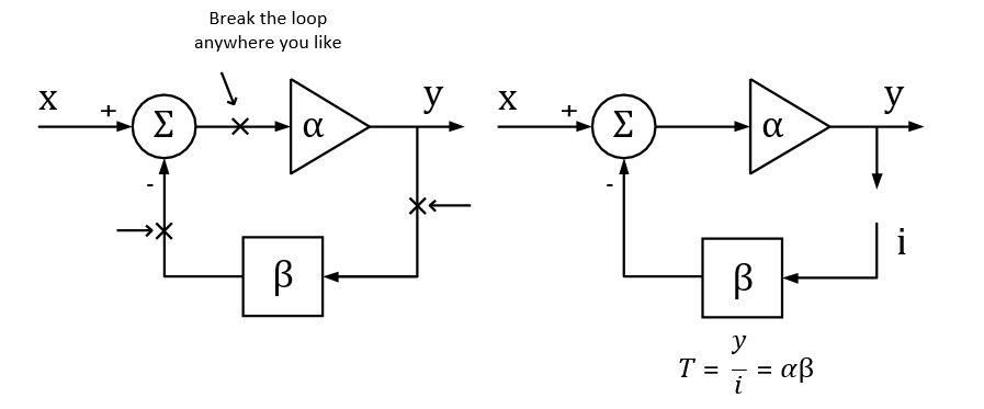 Figure 4: Breaking the loop in a typical feedback system
1.3 Loop Injection
In reality, we can never really break the loop because the feedback loop serves to maintain the DC quiescent operation point of the circuits. Without the feedback loop, the device under test will become saturated because of the small input offset voltage, and then no useful result can be measured.
To overcome this, we should measure the open-loop response inside a closed loop. Therefore, we just inject a signal into the loop rather than breaking the loop. Figure 5 shows a typical method of loop injection. The injection point is chosen so that the impedance looking in the direction of the loop is much higher than that looking backward. One possible point is between the output and the resistor divider feedback network. Other points that meet this requirement may be chosen.
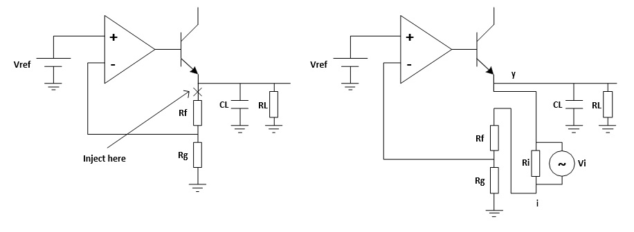 Figure 5: Loop injection
To maintain the closed loop, a small injection resistor Ri is inserted at the injection point. The resistor should be small enough so that it will have little effect on the circuit and also the lower the resistor value the lower the frequency the transformer will operate. Picotest recommends a resistor value of 4.99 Ω for the J2100A, and a larger value may be chosen depending on the circuits. The injection signal is then applied across the injection resistor.
The signal injected should have no effect on the DC operating point of the circuit. A method to solve the common ground connection problem is to use an injection transformer as shown in Figure 6.
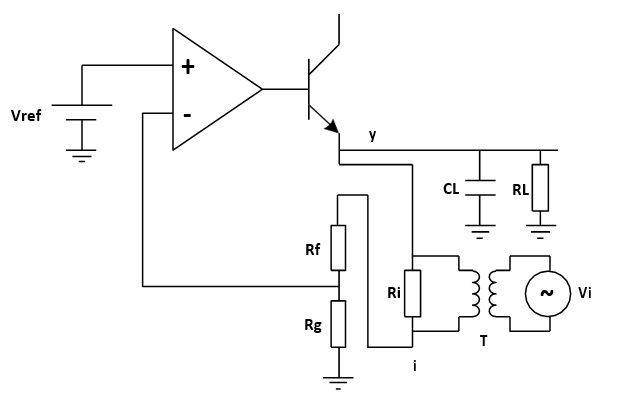 Figure 6: Injection Transformer
The injection signal starts at one end of the injection resistor, travels through the resistor divider feedback network, the error amplifier and the pass element transistor, and finally to the output, which is the other end of the injection resistor. The relationship between the injection signal i and the output signal y is the loop gain that we wish to measure.
Be aware that we are measuring an open-loop parameter inside a closed loop, the phase starts at 180°and decreases to 0°, rather than starting at 0°and decreasing to -180°. So the phase margin should be measured relative to 0°.
2. Measurement Setup and Result
2.1 Equipment
Oscilloscope: Siglent SDS1204X-E with firmware version higher than 6.1.27R1 (Bode Plot Ⅱ release)
Signal Source: Siglent SDG2042X
Power Supply: Siglent SPD3303X
Probe: Siglent PP215 passive probe switched to 1X
Injection Transformer: Picotest J2100A
Device-Under-Test: Picotest VRTS v1.51
2.2 Circuit Connection
The Picotest VRTS v1.51 is a demonstration board for voltage regulator testing. Technically it is a linear regulator built from the famous TL431 and a discrete transistor. The schematic is shown in Figure 7. Different output capacitors can be selected to see the impact on the control loop stability.
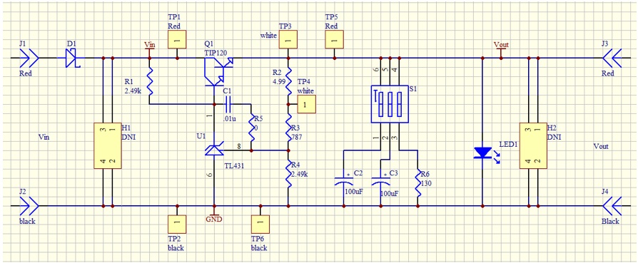 Figure 7: VRTS v1.51 schematic
For the propose of our power supply control loop response measurement, the injection point is TP3 and TP4. The circuit connection is shown in Figure 8.
The generator is connected to the oscilloscope through USB (connection through Ethernet is also supported).
The injection transformer is connected in parallel with the injection resistor so that the signal is injected into the loop while preventing the circuit DC operation point from being affected by the generator.
The TP3 and TP4 points are also connected to the oscilloscope, and the TP4 is defined as the DUT Input while the TP3 is the DUT Output in the Bode Plot Ⅱ.
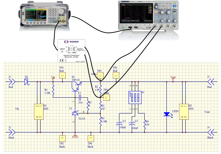 Figure 8: Circuit connection
 Figure 9: Probe and Transformer connections to the DUT
2.3 Instrument Configuration
In this section, we will show how the key configuration should be made in order to make the measurement correctly. For complete instructions to the Bode Plot Ⅱ, please refer to the user manual and the quick start guide.
Before entering the Bode Plot Ⅱ, it is recommended that you enable the oscilloscope’s 20 MHz bandwidth limit setting.
At this time, we want to measure the bode plot from 10 Hz all the way to 100 kHz. This frequency range should be enough for a circuit with an expected crossover frequency at about 10 kHz.
Enter the Config menu and set the Sweep Type to Simple, then enter Set Sweep to set the sweeping frequency. Set the Mode to Decade and Start to 10 Hz, Stop to 100 kHz. Set Points/dec to 20, enough for a typical sweep. Enter the Set Stimulus menu to set Amplitude to 50 mV. Enter the Set Channel menu to set DUT Input to CH1 and DUT Output to CH2.
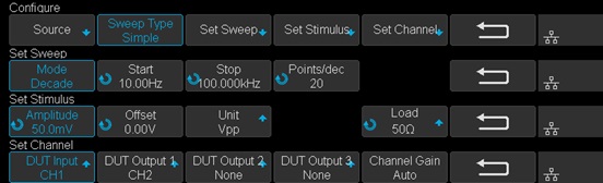 Figure 10: Bode II scope configuration
2.4 Results and Data analysis
After the configuration is done, return to the main menu and press Run to start the sweep.
Wait to see the results as shown in Figure 11.
The result is somewhat confusing and suspect because of the trace at low frequency, especially the phase trace, alternating up and down. We will introduce a method called Vari-level to resolve this problem in the next section.
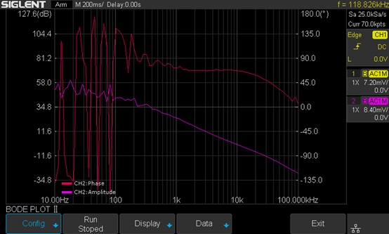 Figure 11: Measurement results
After the sweep has completed, press Run again to stop the sweep. Enter the Display menu and then enter the Cursors menu to turn on the cursors. Use the Adjust knob to move the cursors and set the phase margin as shown in Figure 12.
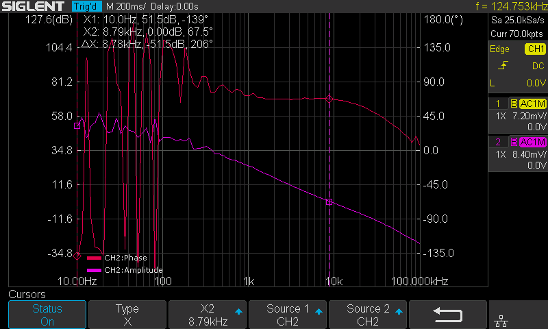 Figure 12: Cursor measurement on the Bode plot
You can also turn on the List feature in the Data menu to examine the measured data, or you can export the data to an external USB FLASH driver for further analysis on a computer.
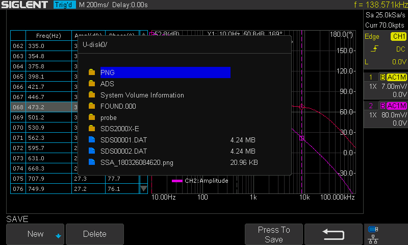 Figure 13: Exporting data
2.5 Vari-level
In the previous section, we can see that the results are not ideal, for the bouncing trace at low frequency. This is because at low frequency the amplitude difference between the input and output channel is relatively large, and since we are using a relatively small stimulus signal (this time 50 mVpp), the signal presented at the DUT Input channel is extremely small so that a commercial general propose oscilloscope cannot measure it accurately.
But we cannot simply increase the stimulus’s signal amplitude. The result will be similar to what is shown in Figure 14. The large signal near the crossover frequency region causes serious distortion to the loop. The distorted signal in the time domain is shown in Figure 15.
Remember that a bode plot only makes sense in a linear system, and has no meaning in a heavily non-linear system. The result is useless.
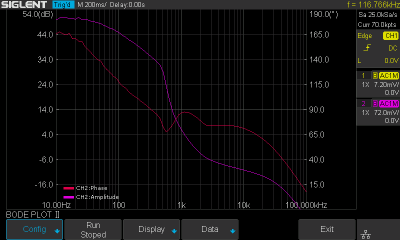 Figure 14: Increased stimulus signal amplitude and distortion
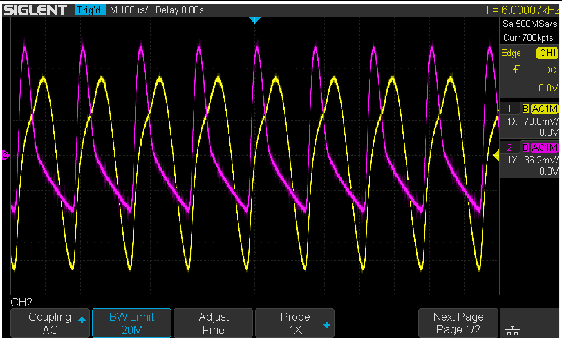 Figure 15: Distortion in the time domain
One possible solution to the problem is Vari-level (other manufactures may call it “Shaped Level” or “Level Profile”). The Vari-level concept is simple: The stimulus signal amplitude is variable over the frequency. If we use a large signal at low frequencies and decrease the amplitude to a fairly small level near the crossover region so that it causes little distortion to the loop, in theory, we can get an ideal result.
Under the Configure menu, set Sweep Type from Simple to Vari-level, and push Set Vari-level to enter the Vari-level profile editor.
 Figure 16: Set Sweep Type to Vari-level
Figure 17 shows the Vari-level profile editor. The Profile option allows the user to select and save up to 4 profiles. The Nodes sets the number of nodes in the profile trace, the minimum allowed number of nodes is 2 because at least 2 points can determine a line, and always the first and the last node set the start and stop of the trace. Press Edit Table will enter the profile editor mode. The parameter under editing is highlighted by cursors, and next push Edit Table again to cycle the cursors between “Freq”, “Ampl” and the entire row, which allows the user to navigate through the entire table. Users can use the Adjust knob to set the highlighted parameter, and pushing the knob will call out a visual keypad that allows direct input to the parameter. The Set Sweep and Set Stimulus option is somewhat similar to that in the Simple type of sweep, but they are not correlated. This time we set the sweep Mode to Decade and a 40-point-per-decade is sufficient. The profile shown in Figure 17 is used in this measurement. It is not the optimum profile for this circuit but should be a good place to start.
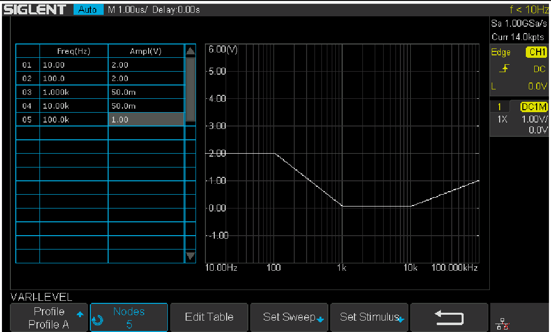 Figure 17: Vari-level profile editor
In practice, one should always experiment with those parameters to find an optimum solution for a particular circuit.
One practical way to do this is to monitor the signal in the time domain, decrease the amplitude of the stimulus signal until no visible distortion can be observed, then decrease the amplitude by another 6 dB. Next, record the amplitude and frequency, jump to another frequency and repeat the process.
There is a better way to find the optimum profile if you already have a known good profile. Reduce the signal amplitude by 6 dB and run a sweep to see if the plot changes. If it does change, reduce the amplitude by another 6 dB and sweep again. Until the result doesn’t change, then you can increase the amplitude by 6 dB and that’s an optimum profile. This is time-consuming but necessary to get a meaningful result.
Once profile editing is completed, return to the main menu and push Run to start the sweep. Figure 18 shows the final result of the measurement with Vari-level. Changing the capacitor selection switch S1 on the VRTS v1.51 demo board will alter the loop response due to the impact of different capacitors.
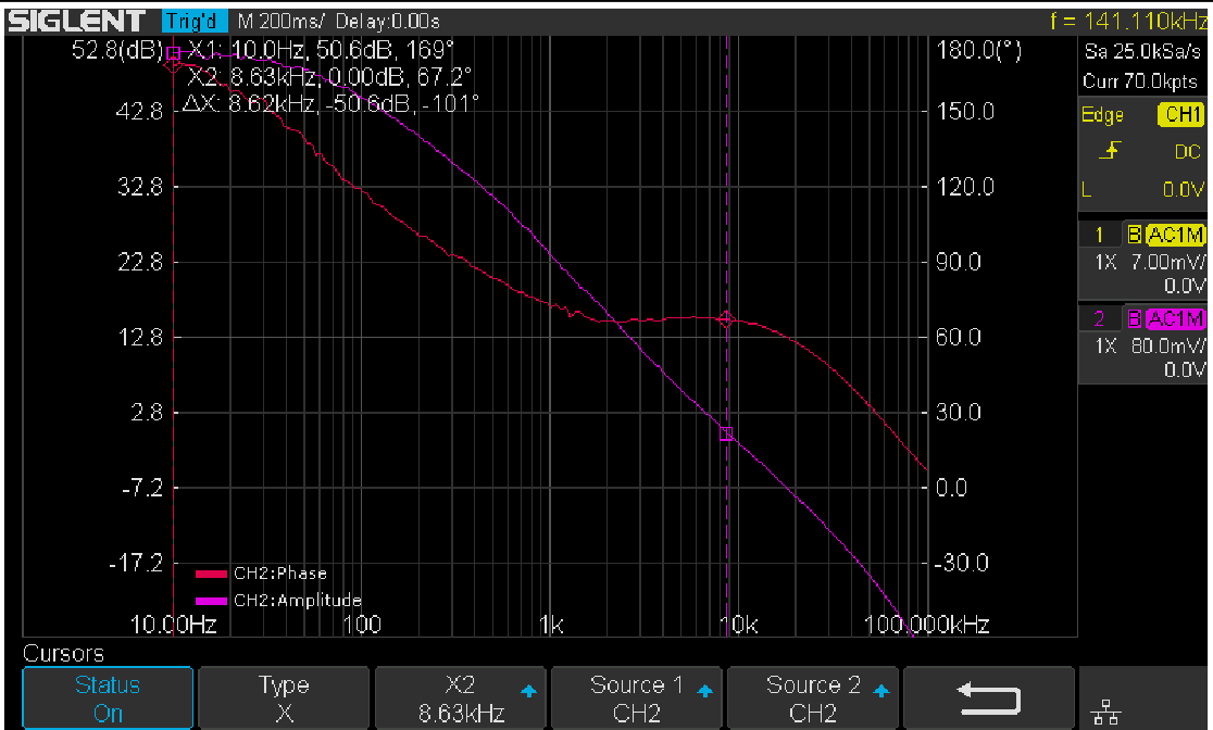 Figure 18: Results with Vari-level
3. Summary
The Siglent oscilloscope with newly released Bode Plot Ⅱ together with a Siglent signal generator and a Picotest injection transformer offer a very flexible and easy-to-use power supply control loop measurement system.
Products Mentioned In This Article:
Measuring the Modulation Index of an AM Signal using an FFT
Introduction
In AM schemes, the modulation index refers to the amplitude ratio of the modulating signal to the carrier signal. With the help of Fast-Fourier-Transforms (FFT), the modulation index can be obtained by measuring the sideband amplitude and the carrier amplitude. In this application note, we are going to show a convenient method of using the new Peaks/Markers function (Available on the 4 channel SIGLENT X-E scopes with firmware revisions > 6.1.31).1. Basic Principle
Amplitude modulation uses a signal (typically a sine wave in the audio frequency range from 10 Hz to 20 kHz) to control the amplitude of a higher frequency signal called the carrier.
A carrier with amplitude modulation can be represented as

Where:
V(t) The Amplitude Modulated Signal
Uc Amplitude of the Carrier Signal
m Modulation Index
a(t) Normalized Modulation Signal
fc Carrier Frequency
Sinusoidal (commonly referred to as a “sine” wave) modulation is the most commonly used modulation waveform type. If we are using a sine wave, the modulating signal can be expressed as

According to the formulas (1) and (2), we can get

 Mathematically represents the carrier waveform.
 and
and 
represent the positive, or upper, and negative, or lower, sidebands of the modulated signal.
The amplitude of both sidebands are

If we set the amplitude of sideband is Us,

In logarithmic case, if the difference between the sideband amplitude and the carrier amplitude is X,

Then the amplitude modulation index can be represented as

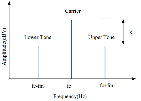
Figure 1
Here, we can see that it is easy to measure the difference between the sideband amplitude and the carrier amplitude, or X. We can then calculate the modulation index very easily.
2. Measurement Setup and Result
2.1 Equipment
Oscilloscope: Siglent SDS1204X-E with firmware version higher than 6.1.31.
Signal Source: Siglent SDG2122X
Cable: 50 ohm BNC
2.2 Instrument Configuration
In this section, we will show how to configure the instruments in order to make the measurement. For complete instructions on the FFT mode, please refer to the oscilloscope user manual and the quick start guide.
The oscilloscope is connected to the output of the signal source as shown in Figure 2.
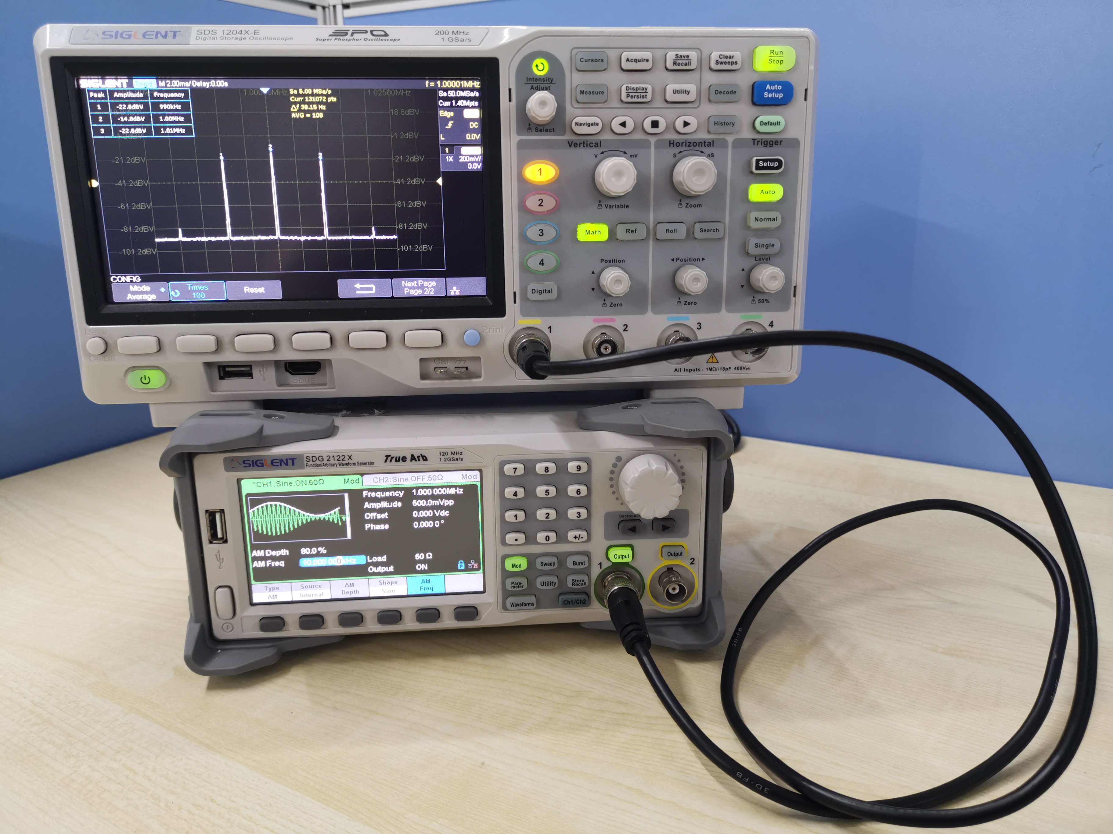
Figure 2 Set Up for the Measurement
The signal source settings are as follows:
- Mod On
- Mod Type: AM modulation
- Carrier frequency: 1 MHz
- Carrier amplitude: 500 mVpp
- Modulation frequency: 10 kHz, and the modulation index is 80%.
According to the output of the signal source, set the center frequency of the FFT plot to 1 MHz and set the horizontal scale to 5 kHz to provide a clear view of the output.
To reduce random errors, the FFT is set to average mode and the average number of times is 100. On the choice of window function, we choose flat-roofed window to obtain the optimized amplitude accuracy.
Starting with firmware revision 6.1.31, the FFT function of Siglent X-E oscilloscopes include a Peaks/Markers function and users can set the number of FFT points separately. The more points the FFT has, the better the frequency resolution of the plot will have. Note that increasing the number of points will increase the time of computation of the FFT, which will reduce the refresh speed accordingly. FFTs up to 1 Mpts at most are available on the X-E series, so we can set the storage depth to 1.4 Mpts. In this application, there is no need for a high sampling rate, since that will lead to a large delta frequency. Set the timebase to 2ms.
According to the input signal, we can deduce that a frame waveform has 28 k-cycles and we will use the first 20 k-cycles to do the FFT operations. For decent resolution, there should be at least five sample points in a cycle, so the minimum number of FFT points should be at least 100 kpts. 128 kpts is suitable, since under the premise of satisfying the measurement conditions, we can get the results faster.
The new version also supports Peaks/Marker, it can quickly identify and label peaks. We choose Peaks to make the measurement.
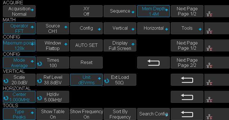
Figure 3 Configuration Screens
The configuration process is as follows:
First, set timebase to 2ms and enter the ACQUIRE menu, set Mem Depth to 1.4M. Second enter the MATH menu, set Operator to FFT, enter the CONFIG menu, set Maximum points to 128k, set Window to Flattop, set Display to Exclusive then go to the next page, set Mode to Average, set Times to 100. Third enter the VERTICAL menu, set Unit to dBVrms, then enter HORIZONTAL menu, set Center to 1MHz, set Hz/div to 5 kHz. Last, enter the FFT TOOLS menu and set Type to Peaks, turn on the Show Table switch to show the peaks list and turn on the Show Frequency switch to show the frequency of peaks, set Sort By to Frequency.
2.3 Result
After configuration is done, enter SEARCH menu, adjust Threshold to show several peaks for easy reading from the table then press Reset. After the average number increasing to 100, the FFT result as shown in Figure 4.
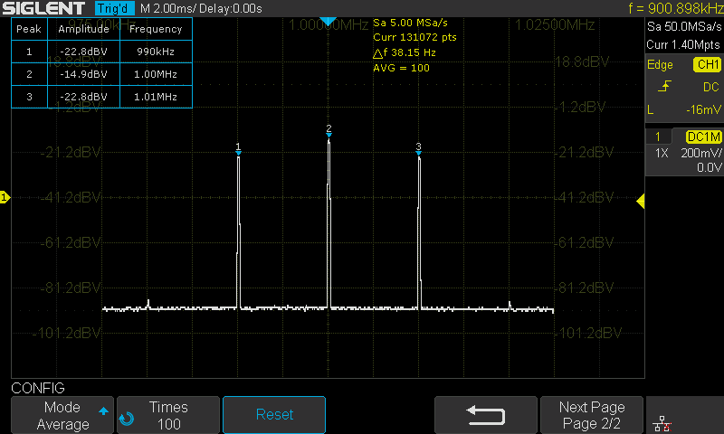
Figure 4 FFT Peaks Result
The carrier amplitude is -14.9dBV, the sideband amplitude is -22.8dBV. So the difference between the sideband amplitude and the carrier amplitude is -7.9dB.
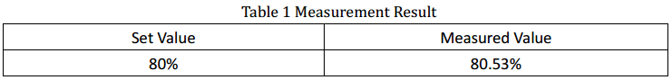
According to the previous introduction, the results of the modulation index are shown in the table 1
3. Summary
The Siglent oscilloscope with newly released Peaks/Markers software, supports peak and harmonic searching which provides a convenient method of spectrum analysis.
Products Mentioned In This Article:
SDS1000X-E Series please see HERE
SDG2000X Series please see HERE
Programming Example: SDS Oscilloscope save a copy of a screen image via Python/PyVISA
Here is a brief code example written in Python 3.4 that uses PyVISA to pull a display image (screenshot) from a SIGLENT SDS oscilloscope via USB and save it to a drive on the controlling computer.
NOTE: This program saves the picture/display image file to the E: drive, which may or may not exist on the specific computer being used to run the application.
Download Python 3.4, connect a SIGLENT SDS Oscilloscope using a USB cable, get the scope USB VISA address, and run the attached .PY program to save an image of the oscilloscope display. The type of file saved is determined by the instruments setting when the program is run.
Tested with:
Python 3.4SDS1102CML+
Products Mentioned In This Article:
Siglent Oscilloscopes please see HERE
Power Supply Design: Load Step Response with a SIGLENT DC Electronic Load
Building a power supply that can handle various loads without oscillating can be a challenge. Computational models and computer simulations can help get your design headed in the right direction, but physical testing is essential to proving the performance of your design.
One method of quickly determining stability is to use a load step response.
In this test, a DC electronic load is used to provide a current load that steps from a low current draw to a higher value in a short period of time. By directly measuring the voltage and current output of the supply with the stepped load, we can visually observe the recovery of the power supply feedback loop and make changes to the design to optimize the response.
For this note, we are going to perform identical tests on two supplies and compare the output voltage and current waveforms: One has been tuned so that the output quickly recovers with minimal overshoot and ringing. The other supply is not tuned and subsequently oscillates. We will also discuss some measurement techniques to help get the right data as quickly as possible.
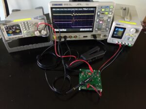
The Equipment:
A DC Electronic Load: The SIGLENT SDL1020X-E is a 200 W load with dynamic testing capabilities to perform the load step. It also features remote sense capabilities to compensate for the voltage drop across the load leads. High currents can provide a substantial voltage drop across the leads and will add unwanted error.
An oscilloscope: The SIGLENT SDS2354X Plus scope has a large display, easy-to-use interface, and features that make capturing these waveforms very easy.
A power supply: The SIGLENT SPD1168X single output supply delivers power to our power supply board
A current probe: The SIGLENT CP4070 features a 150 kHz bandwidth that will minimise most switching noise from the measurement
Power supplies to test: The Analogue Devices LTM4646 series of uModule Regulators. This module features two 10A DC-DC converters. One has been “detuned” to show some common problems associated with power supply design. The other supply has been left in it’s tuned state as a comparison to the detuned supply.The Setup:
- Connect the SPD bench power supply to the power supply to test and configure the output values to match your supply needs. Here, we set the SPD for 12 V @ 3 A.
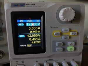
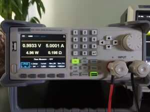
- Connect the SDL electronic DC load to the output of the power supply to test. Configure the load for Constant Current (CC), set the voltage and current ranges to the lowest ranges that still accommodate the requirements of the test, set the current load to a value near the maximum for your design. You may also wish to wire up and enable the SDL remote sense which enables remote voltage measurement to minimize the voltage drop caused by the high current flow through the electronic load leads. Here, we set the current to 5 A.
- Connect a passive probe to the oscilloscope CH1. This probe should be connected to the power supply feedback loop to monitor the voltage as the supply adjusts to the load.
- On the oscilloscope, configure CH1 for AC coupling to provide the most resolution to view the feedback voltage which can have high DC offsets. Enabling the Bandwidth Limit (BW limit) can also decrease noise. Here, the SDS2X Plus also has on-screen labels for traces, which can be a convenient way of keeping information organized. Here, I labeled CH1 Vout.
- Connect the current probe to the oscilloscope CH2.
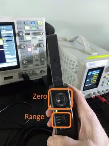
- On the oscilloscope, set the trigger for Rising Edge, CH2 and AUTO. This will allow you to adjust the current probe zero position without dealing with the trigger setting.
- Configure CH2 as a current probe (Units = A), set the Probe attenuation to the proper value (50 mV/A in this case). DC coupling here because we want to see the total signal amplitude. I also applied a label to the output current (Iout).
- Zero the current probe. The CPs have a knob that you can use to move the DC offset. Set the scope to a low current range and adjust the probe to get 0 A on the display.
- Clip the current probe around the positive current lead going from the power supply under test to the DC load. Make sure to have the clamp connected such that positive current flow (into the load) produces a positive signal on the scope.
Now, everything is connected and ready to test:
DC Load Verification
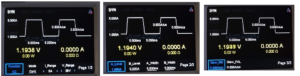
Now, you can power on the SPD power supply and SDL load.Make sure that the scope is set to AUTO trigger for now. You can also add an RMS measurement on CH2 so that you can verify the current draw matches the setting on the DC Load.
Here, we have a setting of 5 A on the DC load.. and we show 5 A RMS on the scope:
Things are looking good. The current output matches our load setting.
DC Load Step Response
Now, set the DC load to Dynamic Current mode by pressing Utility > CC.. and configure the appropriate ranges, low and high current values and duration, and slew rate for your application.
Here are the settings used for this test:
This will continuously cycle from 1 A for 5 ms to 5 A for 5 ms with 500 mA/us slew rate.
Now, switch the scope trigger mode to Normal and adjust the vertical, horizontal scales and positions.. as well as the trigger level to get a stable trigger and a few periods of transition on the display:
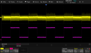
Verify that the supply high and low current values match the setpoints. For this example, we have 1 A for 5 ms and 5 A for 5 ms.. which is what we observe.
Observe and Optimise
Now, let’s compare a tuned setup to one that is not tuned for our load as well as some techniques to gather more information about the response.
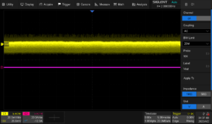
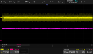
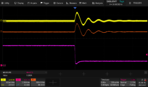
First, you likely see quite a bit of noise on your signal. The majority of this is due to switching noise in the supply being tested. Here is a zoomed image of the feedback voltage where you can see the switching noise quite clearly.
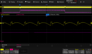
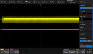
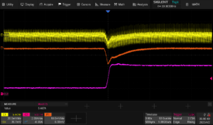
Enabling waveform averaging can help:
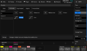
Now, we see the output voltage from CH1 (yellow), output current from CH2 (pink/purple), and the average voltage math function (orange):
This is the tuned setup.
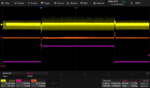
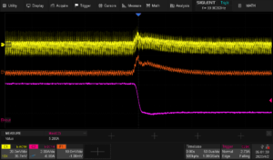
Now, let’s look at a detuned supply:
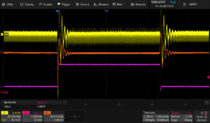
The scaling on these two images is exactly the same. You can see a large amount of ringing associated with the detuned supply. This design is very close to becoming an oscillator with this load. If our step duration was any shorter, the supply voltage wouldn’t be settled and our output would be very poorly regulated.
Here are some closer images of the rising and falling edges on shorter time scales:
Tuned, Rising:
Tuned, Falling:
Detuned, Rising:
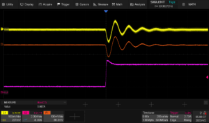
Detuned, Falling:
Conclusions
A DC load step test can quickly show you the performance and stability of a power supply design. Using a few common pieces of test gear, you can ensure that your design is ready to undertake the most challenging application requirements.Creating an arbitrary IQ Waveform using MatLAB and UltraIQ
Introduction
The DSG3000 (DSG3000B) Series RF signal source (Figure 1) is designed for RF engineering and signal development and test up to 6 GHz. The instrument is also capable of a number of modulation formats. One of the more advanced capabilities is IQ modulation that is enabled with the DSG3000-IQ option. This option adds both a baseband generator and the ability to externally generate IQ modulation for the carrier. The baseband generator’s I & Q data can also be directly output for additional verification and testing. Rigol’s Ultra IQ Station Software (Figure 2) makes it easy to generate standard IQ signals and load them into the instrument, but many engineers are now working with advanced, custom data or are experimenting with new modulation schemes for IQ data altogether. For these applications, Rigol has developed the following code examples for taking I & Q data in Matlab and delivering it directly to the instrument natively from within Matlab.
This guide will demonstrate how to install and configure the Rigol Matlab code as well as run several examples that load data into the instrument. We will then show the results using our DSA875 Spectrum Analyser (Figure 3) on the modulated carrier and our DS2000A Series oscilloscope on the baseband outputs.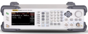
Figure 1: Rigol DSG3060 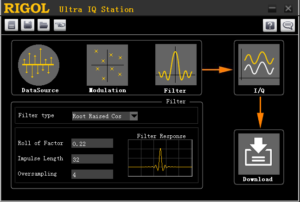
Figure 2: Ultra IQ Station Software 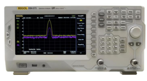
Figure 3: Rigol DSA875 Installation and Configuration
Required components
There are several requirements for running the example code. We have tested the example code on the current version of Matlab as of this writing which is R2014b. First, download the Rigol custom IQ example here. The example code combines C++ to create the binary data streams with LabVIEW and VISA that handle the instrument communication. That code needs to be accessed from the Matlab command window. To achieve that several items may need to be installed in your system:
1) Microsoft Visual Studio C++ 10.0 and the Windows SDK 7.1
2) LabVIEW runtime engine for 2013 for your OS
3) VISA which installs with Rigol’s UltraSigma
Details:
1) The Microsoft tools are required to access the compiled C++ code that encodes the Rigol IQ data streams. Go here for the Matlab answer for installing these components to work with Matlab. Read the entire answer as there are different installation plans depending on what you currently have installed. Once you have installed the Microsoft tools you can verify the compiler settings from within Matlab by following these steps:
• Open Matlab
• Browse to the Rigol Custom IQ Example folder (Figure 4)
• In the Command Window at the prompt type ‘mex –setup’
• Matlab will respond with its current compiler settings. These responses are acceptable:
• Microsoft Windows SDK 7.1 (Figure 5)
• Microsoft Visual C++ 2010 (Figure 6)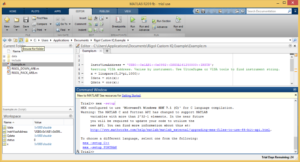
Figure 4: Matlab window with Browse button highlighted and a mex –setup response in the command window 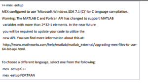
Figure 5: Text from a Matlab mex –setup response related to the C++ compiler settings using SDK 7.1 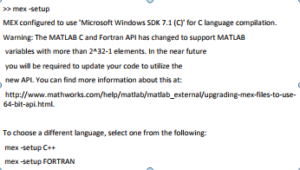
Figure 6: Text from a Matlab mex –setup response related to the C++ compiler settings using Visual C++ 2010 If Matlab is using some other compiler or has yet to select a compiler follow the links and information in the mex –setup response to configure one of these compilers. The example code may or may not work correctly with other compiler settings.
2) Download and install the NI LabVIEW runtime 2013 applicable for your operating system.
This download may require you to register at ni.com and the PC should be rebooted after installation. The example code has been tested on 64 bit and 32 bit systems. All of the required components are available for other OS options as well, but this example was not developed or tested for those environments.
3) Install Rigol UltraSigma. Download it here. It is a 522 MB file that includes the required VISA drivers. It is also helpful for identifying your DSG3000’s VISA address quickly and easily. That download include installation and usage guides for UltraSigma.
Connecting your DSG3000
Plug in and power on the DSG3000 signal source. Push the green PRESET button on the left to reset it to the default conditions. Now connect the USB Device port on the rear panel to the PC running Matlab. The DSG3000 can also connect over Ethernet or GPIB, but we will focus on USB communication.Then, Run UltraSigma and you will see the DSG3000 appear in the Resource list (Figure 7). The string in parentheses after the model number is the VISA resource string. This is the string we need to edit in our Example.m file. To copy the address right click on the instrument model number and select Operation Copy Address (Figure 8). Now we will edit the Example.m file in Matlab to have the correct resource address for our connected instrument. In Matlab, right click on Example.m in the Current Folder window and select Open. The file will now open in the editor. In the first line of code InstrVisaAddress is set equal to a string in single quotes. Highlight the string leaving the single quotes and paste the string we copied from UltraSigma. This Matlab view is shown in Figure 9. Once this is complete save the Example.m file. Repeat the paste and save process on Example2.m for later. We are now ready to run the examples. Remember, the DSG3000 must have the DSG3000-IQ option enabled to accept these commands.
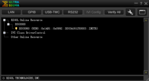
Figure 7: UltraSigma showing DSG3000 connected 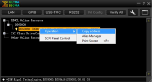
Figure 8: UltraSigma address copy function 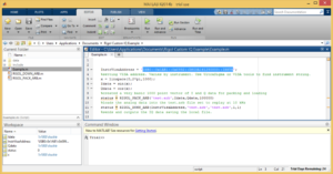
Figure 9: Example.m editing in Matlab Creating Custom IQ data
This example creates the simplest IQ data stream by encoding the I data as sine and Q data as cosine:
InstrVisaAddress =
‘USB0::0x1AB1::0x0992::DSG3A161250003::INSTR’; x = linspace(0,2*pi,1000);
Idata = sin(x); Qdata = cos(x);
status =
RIGOL_PACK_ARB(‘test.arb’,Idata,Qdata,100000); status = RIGOL_DOWN_ARB(InstrVisaAddress,
‘test.arb’,’test.arb’,1,1);
First, we set the VISA resource address. Then, we create arrays of data for I and Q. Next, we pack that information into a binary file and then we finish by sending that data to the instrument.
There are 2 custom commands that call Rigol compiled code:RIGOL_PACK_ARB
This command converts I & Q data arrays into a local arb file that can be loaded directly to the instrument. The file describes both the data and the desired playback speed. [ status ] =
RIGOL_PACK_ARB(LocalFileName,Idata,Qdata,SampleRate) Definition:
• LocalFileName is the local file to create on the computer. MUST end in .arb• Idata is the vector of real numbers representing the I data over time. Values should be -1 to 1.
• Qdata is the vector of real numbers representing the Q data over time. Values should be -1 to 1.
• SampleRate is the real number representing the number of samples to put out per second. Default is 100 kSa/sec or a 100 kHz sample rate, so the units is kHz. Value can be set from 1 to 50000. 100000 can also be discreetly set.
Status returns 0 for success and 1 for a failure to pack the file.
RIGOL_DOWN_ARB
This command downloads a local arb file created by RIGOL_PACK_ARB to a connected DSG3000 instrument and optionally enables the output.
[ status ] = RIGOL_DOWN_ARB(InstrVisaAddress, FileNameOnInstr, LocalFileName, OutputEn, KeepLocalFile)
Definition:
• InstrVisaAddress is a string representing the VISA resource name for the DSG3000 you want to load the file to. Typical string would look like
‘USB0::0x1AB1::0x0992::DSG3A1301080006::INSTR’ for a USB resource.
• FileNameOnInstr is the file name to give the wave on the instrument. It MUST end in .arb. This filename is changed to all capital letters in the instrument.
• LocalFileName is the file name created during the PACK procedure. It MUST end in .arb
• OutputEn is the output enable option. Send 1 to automatically load and output the file. 0 does not enable the output. 1 is the default.
• KeepLocalFile determines what to do with the local file on the computer after loading is complete. Send 1 to automatically save the file. 0 deletes the file. 1 is the default.
Status returns 0 for success and 1 for a failure to pack the file.
Tips:
File names do not support paths. Use files directly. Getting active output may require setting of RF, MOD, and or IQ SWITCH to ON. Verify these are active when trying to view output signals.Custom IQ Test and Verification
Now that we have explained the functions we can run the examples provided. The first example, which we have already discussed, creates a simple sine wave and cosine wave in the I & Q data respectively. We test and verify this with our DS2000A Series oscilloscope. First, connect the Baseband I & Q outputs on the rear panel of the DSG3000 to the channel 1 and channel 2 inputs of the oscilloscope. I out should be connected to channel 1. Q out is connected to channel 2.
Then, run Example.m by right clicking on the name in the current folder window in Matlab. Select Run from the popup. The code will execute and after a few seconds the outputs will appear on the oscilloscope. You can reset the DS2000A oscilloscope to the factory defaults:
• Push Storage
• Select Default
Then, from the factory settings Push AUTO. For our purposes we want to see the relationship in phase between I & Q. While it is a simple comparison because the sine and cosine are 90° out of phase, it is still instructive to view in XY mode. Push the HORIZONTAL MENU button and under TIME BASE select XY. By adjusting the channel scales and offsets you can center that image to get to Figure 10. This view is relevant because it is similar to a basic constellation decoding view used for signals encoded with phase information.
Lastly, we can run Example2.m the same way. This file generates IQ data that traverses a basic 4 x 4 constellation diagram and repeats as shown in Figure 11.
If we connect the DSA875 to the RF output and mix this data onto a 6 GHz carrier by setting the DSG3000 Level to -10 dBm, turning on the RF and MOD lights, and turning the IQ Switch to ON we can view the occupied bandwidth of the signal. The IQ data from Example2 has the spectrum shown in yellow on Figure 12. If we change the SampleRate in the RIGOL_PACK_ARB command from 10 kHz to 1 MHz and run it again the spectrum is now the purple signal in Figure 12.
Therefore, with our DSG3000 RF signal source,
D2072A oscilloscope, our DSA875 spectrum analyser, and our Matlab examples we can create our own custom IQ data, test, and verify the basic IQ constellation patterns as well as compare spectrum usage making a good start on our exploration or advanced RF modulation schemes.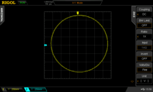
Figure 10: Scope XY mode view of I and Q baseband signals showing phase relationship 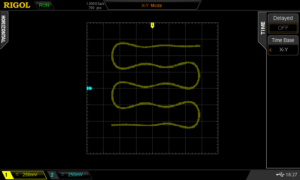
Figure 11: Scope XY mode view of Example2.m 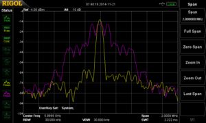
Figure 12: DSA875 showing the Example2 modulated signal at 10 kHz and 1 MHz IQ symbol rates Products Mentioned In This Article
Precompliance: Susceptibility testing
EMC Precompliance Testing: Immunity/Susceptibility
Solution: Products that contain electronics can be sensitive to radio frequency (RF) interference. Devices that experience RF interference can be prone to improper or failed operations. Products that suffer problems when exposed to RF interference are said to be susceptible to interference while products that do not exhibit issues when exposed to RF interference are said to be immune to interference.
RF interference can cause:- Scrambled display information
- Slow, Frozen, or locked operations (no response from keys, knobs)
- False or noisy data
- System reset or reboot
Design analysis, including part selection, shielding, and cable selection is the first step in creating a product that is capable of operating “as expected” under a certain degree of RF interference, but testing early under real world conditions is one sure way to determine if your design is susceptible to any issues with RF.
In this application note, we are going to show you how an RF generator and some simple tools can help you identify weaknesses in your product design.
A Word about Precompliance
Most governments have regulations in place that specify the amount of electromagnetic interference (EMI) a product can emit into the environment (radiated emissions) and conduct down the power cord (conducted emissions).There is also an increasing number of regulations that cover how much EMI a product can endure from outside sources (susceptibility).
Products being sold within the areas covered by these regulations must comply with the defined test limits. Compliance tests use these regulations to define the proper instrumentation, physical setup, and experimental techniques and experience to correctly record and report properly. This testing is very important and required for legal sale of the product within the covered area. Unfortunately, compliance testing can be expensive and difficult to execute due to the specialised equipment and knowledge required to properly conduct the tests.
Precompliance testing simulates the major details of a compliant test setup at a lower investment in time and money. Before you go to a compliance lab for testing, you can use precompliance tests to gather information about the performance of a design, make changes (if needed), and retest.. all in an effort to minimise the return trips to the compliance lab.
A word of caution, however. Precompliance data can be useful in hunting down many, if not all, of the non-compliant areas of a design but it is not a substitute for testing at a fully accredited compliance lab. Ultimately, the company (you) is responsible for proof of compliance to the full regulations for your product.
Radiated Susceptibility
Radiated susceptibility tests involve observing the operation of a device-under-test (DUT) while it is being subjected to a known RF source. The signal is delivered to the DUT using antennas for far-field testing or near field probes for board level tests.
Most radiated susceptibility regulations are based on IEC 61000-4-3 which defines the test signals range from 80-1,000MHz. This signal can be modulated by a 1kHz AM sine wave with 80% modulation depth. The modulated signal helps to quickly identify any rectification issues within sensitive circuit elements.In far-field tests, an RF signal source, like the Rigol DSG3000 or DSG800 series is connected to an antenna that is set up a meter or two from the DUT. The RF source is then configured to source an output with 80% AM modulation at 1kHz. The amplitude should be set as high as possible, and the carrier frequency can be set at 9kHz.
NOTE: The DUT should be configured in its most commonly used state. All cabling (power, I/O, etc..) should be connected and in place. Cables can act like antennas and can directly influence performance.
Observe the DUT for any functional changes or issues such as a glitching or noisy display. Now, increase the carrier frequency and check the DUT. Step the center frequency of the generator and continue to observe the DUT, making note of the carrier frequencies that cause issues and the type of problems observed. After you have completed stepping up to 1GHz, you can rotate the DUT with respect to the antenna and re-test if you desire a more thorough test.
NOTE: Antennas and should only be used in shielded anechoic or semi- anechoic chambers to prevent interference with communications and emergency broadcast bands. It is illegal to broadcast over many frequency bands without proper licensing.
The use of an RF source like the Rigol DSG3000 (DSG3000B) or DSG800 series allows you to the flexibility to adjust the wavelength, power, and modulation of the output to help identify problem areas quickly.
Figure 1: The Rigol DSG800 and DSG3000 RF Source. 
Figure 1: The Rigol DSG800 and DSG3000 RF Source. Near Field testing is helpful because it does not require specialised chambers for testing. The E and H field probes only produce strong fields at distances less than 1” from the tip of the probe and do no radiate efficiently enough to cause problems with broadcast and emergency systems. Their small size also allows you to pinpoint the RF at specific circuit elements.
Figure 2: RIGOL’s NFP-3 set of Near Field Probes. These are all H field probes. The RF source is configured exactly as in the far-field test, but this time, the probe tip is placed very close to the circuit or elements of the board at each carrier frequency. As you scan across the circuit, observe the DUT and be sure to check for any issues. Especially near sensitive analogue circuitry.
In the figure below, we removed the shielding from an oscilloscope board and used a probe and DSG3000 to deliver RF signals into the sensitive analogue front end. As you can see, with the shielding removed, the RF causes data corruption and changes the waveform significantly.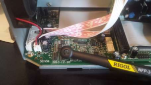
Figure 3: Using a near field probe on an unshielded Oscilloscope analogue input circuit. 
Figure 4: Oscilloscope data with shielding in place. 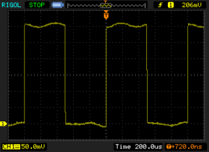
Figure 5: Oscilloscope data without shielding. Additional testing
Another useful test technique is to use a current probe and RF source to deliver RF signals to cables connected to the DUT. Cables can act like antennas and couple undesired signals to the DUT. You can use this setup to step through different frequencies and check the susceptibility of your design. Commercial current probes can be used.. but an acceptable current probe can be built using a snap-on ferrite choke, a few winds of insulated wire, some epoxy, and a BNC connector as shown below: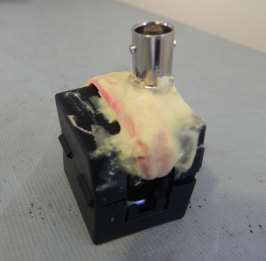
Figure 6: Homemade current probe. Simply setup your DUT and connect all of the cables that are common to its usage. Configure the source to output maximum power with the same 80% 1kHz AM modulation that was suggested for far and near field tests earlier and observe the DUT for problems. Step the carrier frequency and observe. Perform this test to the maximum desired frequency and repeat the process on each cable used with the DUT.
NOTE: Clamp probes should only be used in shielded anechoic or semi- anechoic chambers to prevent interference with communications and emergency broadcast bands. It is illegal to broadcast over many frequency bands without proper licensing.
To demonstrate the use of a current probe, we performed an experiment on a USB powered demonstration board. We used a DSG3000 and a homemade probe clamped to a non-filtered USB cable connected to the board and we monitored the output signal.
Figure 7: Injection of RF to an unfiltered USB cable. With no RF applied, the data was smooth.
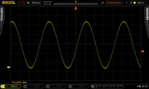
Figure 8: Sine wave from board without RF interference. But, when an RF signal was applied, the output began to show signs of interference. The worst interference occurred at a carrier of 110MHz, as shown below.
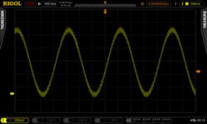
Figure 9: Noisy data showing RF interference at 111.1MHz due to injected noise. In conclusion, an RF source like the Rigol DSG3000 or DSG800 and some simple tools can enable you to test your designs for immunity issues early in the development process. Saving your company time and money.
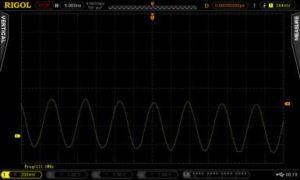
Figure 10: Zoomed data to show details. Products Mentioned In This Article:
VNA Measurements Application Note
Basic measurements with a Vector Network Analyser
In our wireless world the need of RF component testing is one of a key factors to bring a product to market. Devices are getting smaller and are containing more and more complex components. It is a must to have knowledge of complex impedance (or admittance) and reflection / transmission parameters to bring the most optimum functionality to the RF device. RF components like filters, resonators, etc. can be calculated according to capacitance and inductive values. Software simulators can take these values and help fine tune the design. But at the end of the day, the quality and performance needs to be measured. For several applications, a scalar network analyser might be adequate but for some specific design work phase information is required. A vector network analyser [VNA] has the possibility to measure amplitude and phase over specified frequency range.
The vector network analysis allows for the measurement of complex scattering parameter [Sxx] of a device under test [DUT] over a specified frequency range. Vector network analysis allows for the characterisation of a scattered matrix with reflection [S11] and transmission [S21] factors. These parameters are required to design e.g. a matching circuit for an amplifier. With phase information it is also possible to calculate the time range where additional failures at different positions can be analysed. Due to the complex (vector) characteristic it possible to make an accurate correction with calibration routines.
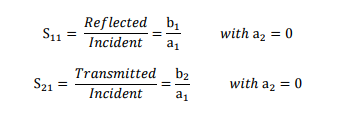
RIGOL’s VNA solution in RSA5000N and RSA3000N [RSAxN] series can perform three different measurements these include reflection [S11], transmission [S21] and Distance-To-Fault [DTF] measurements. All three of these measurements have several different views which allows engineers to easily determine a DUT’s frequency response, phase, SWR, Smith Charts and Polar Plane measurements. In figure 1 the principle of S-Parameter measurement is visible. These parameters can be calculated with the complex factors ax and bx. For example, a1 refers to the incident wave into the DUT and b1 refers to the reflected wave. The transmitted factor after DUT is referring to b2. At RSAxN version an incident wave can only be generated by port 1. Therefore, a2 is 0.
The principle of S Parameter Measurement in a network: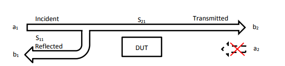
S11 Measurements
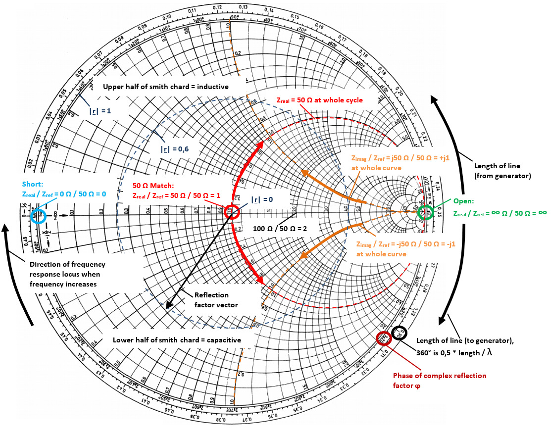
The reflection measurement is an important key to specifying the performance of complex systems (e.g. wireless communication system) Reflection factor r describes the ratio of incident and the reflected wave. There are several different tools that can be used to perform this measurement but one of the most useful tools is the Smith Chart because it contains the most information, like:
• Complex impedance and tools to determine how to match the (compensation of inductive / capacitive reactance)
• Complex reflection factor
• Impact of real / capacitance or inductive
• Influence of frequency range and displaying frequency response
• Q Factor of RF components
• Influence of the cable length
• Determination of cable loss
In RSAxN the Smith Chart can display impedance [Ω] (components in series) or admittance area [1/ Ω] (parallel connection of components). A universal Smith Chart is visible in figure 2. “Universal” means it can be used for each system impedance. In this example a 50 Ω reference is used (which can be modified to a different impedance, like 75 Ω if required). The reference is used to center the chart for better visualisation. A complex impedance of Z = 50 Ω + j25 Ω is transformed with that reference into 1 + j0,5 to make manual calculations easier. But in the end the calculation for real complex impedance has to be done after the measurement has been finalised. In RSAxN it is possible to measure the transformed values via a marker and display impedance value (in the example above: 50 Ω + j25 Ω).
Taking into consideration to have a serial connection of impedance, capacitance and inductivity, the impedance is calculated as follow:In this formula it is visible that the inductive imaginary component is positive and capacitive imaginary component is negative. The lower half of Smith Chart is referring to capacitance and upper half is referring to inductance. On the outer diameter of Smith Chart, the length of line referring to Wavelength λ is displayed. On the Smith Chart it is visible that a turn of 360° results into 0.5 x l/λ. The second value which is visible on the outer diameter is the angle ϕ of a complex reflection factor r. There is a 100% reflection of incident wave with either an Open termination (right side of the chart; when the real and imaginary impedances are close to ∞ Ω) or with a Short termination (left side of the chart; when these impedances are closed to 0 Ω). In the center of Smith Chart the impedance of 50 Ω is visible. It is possible to measure out the complex reflection factor in Smith Chart, but it is easier to use a marker in the Polar Plane in RSAxN to get this value.
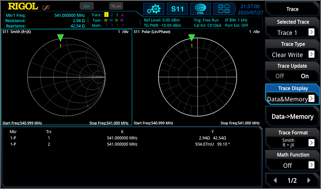
The Smith Chart and Polar Plane are useful tools to analyse complex impedance and reflection factor on a network for a specific frequency range. In figure 3 the capacitance in series with a resistor was measured at 541 MHz. The same configuration was measured again with a cable at ~16 cm. In this example it is visible that the impedance position is changing when using an additional cable at a specific frequency. The reflection factor remains very close to the origin point (cable has attenuation which has for this measurement a very small influence. As higher the cable attenuation, the more their has influence).
The marker on the Smith Chart calculates the correct impedance when using the reference of 50 Ω. Then the same configuration was tested again without the additional cable over a different frequency range (see figure 4).
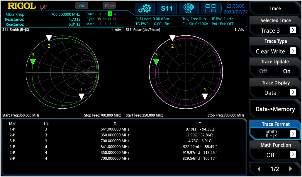
In this measurement the frequency response curve is visible for the adjusted frequency range. With the marker it is visible that the curve is moving clockwise with increasing frequency. In RSAxN version different intermediate frequency bandwidth [IF BW] can be used for testing (1 kHz to 10 MHz in 1-3-1 steps) to realise the frequency resolution as required.
For complex networks one of the top uses is of the impedance to the network (here: to realise 50 Ω at network input) at the required center frequency. Different possibilities can be used in which can be shown on the Smith Chart.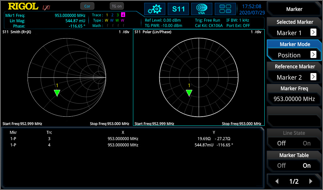
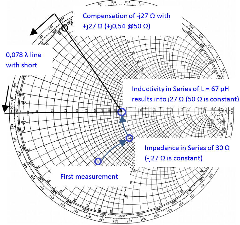
First, with a series impedance of 20 Ohm can be set to 50 Ohm. As a next step an inductive component in series could be used to bring the impedance level to 50 Ω without an imaginary component (see figure 5). The problem of this theory is that the inductive component (in this case: 67 pH) is very small and hard to realise. Discrete inductive or capacitive elements can only be used for maximum frequency of several 100 MHz. For higher frequency ranges, different methods (e.g. microstrip solutions) needs to be used. One of the approaches might be using a serial 50 Ω stub to compensate the -j27 Ω (length of stub with short: l = 0,078 λ, with open: l = 0,328 λ). For the stub, the dielectric constant is required to evaluate the correct wavelength.
For S11 it is also possible to display return loss and (voltage) standing wave ratio [(V)SWR] over frequency range. If “V” is used, then the ratio is defined to voltage level of a standing wave at a line.
VSWR is referring to the maximum and minimum voltage values that is being transmitted and reflected by the component. The difference to reflection factor is, that there is no relation to phase.For deeper analysis it is often necessary to use logarithmic values to have a deeper view of smaller modification compare to bigger values. In RSAxN it is also possible to display the return loss value ardB in log scale over the frequency range.
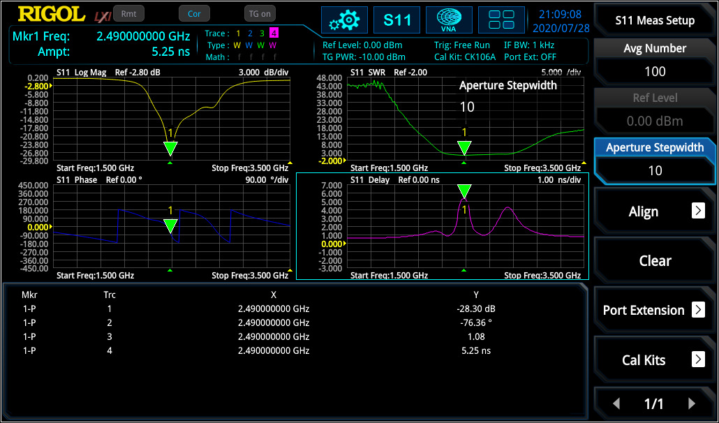
Linear distortion occurs in all linear networks and components. Linear distortion could have an impact deviation in phase, in amplitude and / or in a constant group delay. When measuring a filter with the RSAxN, it is possible to measure amplitude flatness, the deviation in phase and group delay (Group delay is a deviation from linear phase). Thereby the VNA using phase over frequency and adds it to a positive constant phase over frequency. The difference of both results is the phase deviation over frequency and the group delay is calculated as follow:
Each signal will be delayed with transmission over a component like a filter, amplifier, etc. different group delay results in a non-linear delay of signals at different frequency components and distorts the signal, which is not ideal and not desired. If the group delay is constant over the frequency range, all frequency components will have the same shift and, in that case, the ideal system would be free of distortion and the group delay would be a constant value. The aperture step width [df] can be adjusted in RSAxN according to their need. In S11 (and S21) measurement of RSAxN, phase and group delay can be measured and displayed over the desired frequency range (see figure 7).
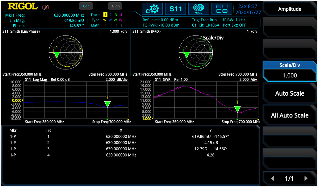
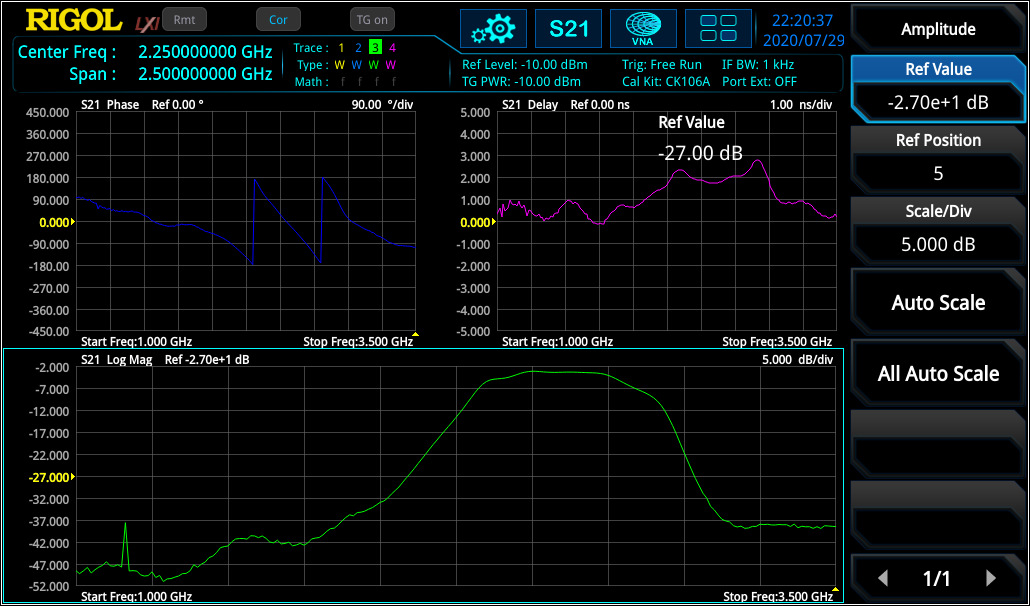
S21 Parameter Measurements
S21 parameter defines the insertion loss over a specified frequency range which can be measured with high accuracy after a Through calibration. The measurement of frequency response can be used to measure the 3 dB bandwidth of a bandpass filter (see figure 8) or characterise amplifiers.
Similar to S11 measurement, also phase over frequency range and group delay can be measured with RSAxN (see figure 9).
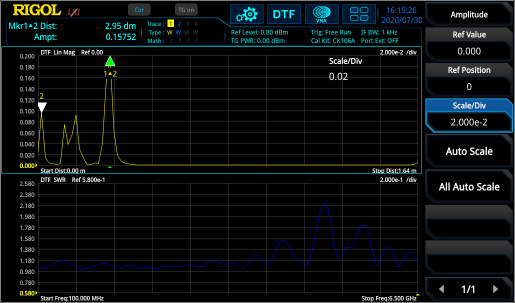
Distance-to-Fault Parameter Measurements
In RF measurement normally frequency range will be selected because it has more significance in characterisation in this area. For example, a filter will be characterised in frequency range. But for some cases it is very useful to take also a look into the time range to evaluate impulse response of a DUT.
One big advantage when phase information is available is, that the frequency range can be transformed (via Inverse Fast Fourier Transformation [IFFT]) into time. The time view has different advantages, it can be used to localise a defect on cables due to measurement of impulse response, localisation and characterisation of discontinuities or getting a better view of physical characteristic of a DUT. In the formula below it is visible that S11(t) is the impulse response of reflection factor S11(ω):Figure 10 shows the frequency range (S11) and DTF measurement of a DUT (two cables with connectors in between and a 50 Ω match at the end). In the frequency range, the discontinuities can only be captured in summary. But in DTF the reflection points are easily visible and can the exact distance of reflection points (e.g. due to connectors or cable defects) can be measured with marker. It is necessary to perform the same calibration like for S11 measurement.
Calibration
One important part of accurate measurements is the calibration procedure. Each measurement contains different failure mechanisms, with calibration routines these can be minimized, and the quality of measurement accuracy can be increased.
S11 / DTF Calibration:
D = Directive Error: coming from imperfect signal split of coupler.
MS = Source Match Error: coming from imperfect source matching of VNA
TR = Tracking Error: coming from frequency response of components used for signal split (like directive coupler) and mixer and internal detector.
Here is an error model for a one port measurement: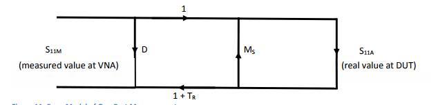
Load calibration: With using a 50 Ω impedance [load], S11A is 0 and S11M = D (Directivity Error from directivity coupler is measured). VNA is now minimising the directivity error [D] over the adjusted frequency range. After this calibration, the directivity error of RSA5000N is ~40 dB.
Short / Open calibration: From the DUT’s view there is a mismatch of source [MS] which creates a reflection loop between the DUT and the system. This failure is visible when the DUT shown a mismatch. Additionally, the frequency response failures [TR] due to connectors, cables, internal coupler, detectors occurring. With open (S11A = 1) and short (S11A = -1) calibration there will be two equation with two factors Ms and TR and the VNA knows these values.
The calibration standards Open / Load / Short and Through should be ideal to reach e.g. with Short r = -1, but they aren’t. E.g. an Open contains stray capacitances or Short contains inductivities. This is not a problem, when the non-ideal behaviour of standards is known. For RIGOL’s calibration kit CK106A (DC – 6.5 GHz) and the CK106E (DC – 1.5 GHz) the parameters are known and already integrated into the RSAxN versions. With regards to these values an accurate calibration is now possible. If an additional calibration kit is used, then these parameters needs to be customized according to this kit.
For DTF measurement, the velocity factor of cable (e.g. 70% 0.7) and the cable loss needs to be integrated to extend the accuracy of the measurement. Both values are defined in cable specification.
S21 Calibration:
For S21 (transmission factor) measurement, a Through calibration is required to flatten the frequency response of cabling and connection (needed to connect DUT to VNA) from VNA source to VNA input. Figure 13 displays the curve before and after Through calibration.
The RSA5000N and RSA3000N series have four additional application modes, in addition to the new VNA function. These four modes include RTSA (real-time spectrum analyser up to a maximum bandwidth of 40 MHz), GPSA (sweep-based spectrum analyser with outstanding performance), EMI (pre-compliance tests according to CISPR specifications) and VSA (vector signal analysis for different digital demodulation and bit error measurement, only RSA5000N). With the addition of the VNA application mode the RSA5000N and the RSA3000N series are some of the most complete RF testing platforms on the market.
Products Mentioned In This Article:
Real-Time vs. Swept Spectrum Analysers
Real-Time Spectrum Analyser vs Spectrum Analyser
Today the RF industry has to face more and more the open question, how to transport the data from my test device (DUT) to different receiver spots (like to transmit data into World Wide Web). For IoT applications the most common way is, to use wireless transmission of data via common standards like Bluetooth, Wi-Fi or Zigbee. A more complex test system than a spectrum analyser is required to evaluate the results in a short time. Wireless transmission works with digitalisation of data. These digital data will then be modulated to an RF carrier via complex modulation schemes. This process results in a very fast and dynamic signal change over time and frequency band. Speed becomes more and more an important factor in frequency analysis. So it is not enough to use a sweep based spectrum analysers with FFT or superposition principle. Rigols new outstanding Real-Time Spectrum Analyser RSA5000 series will give the answer to that question and combines an elegant design with full flexibility and speed during test.RSA5000 series can be switched between a common superposition spectrum analyser [SA] and a real- time spectrum analyser [RT-SA]. The RSA5000 is working like a SA of the DSA800 series but with better RF performance. This document will describe the difference of analyser techniques and will display the advantages:
The complete RF input signal will be set to an intermediate frequency via a swept local oscillator in superposition technique. In other words a signal trace of SA will be sweep between start / stop frequency according adjusted center frequency and span. Sweep time is depending of adjusted parameter like RBW, VBW, Span. This measurement technology can be perfectly used to get a fast overview of a wide range spectrum with good amplitude accuracy and for insertion loss or VSWR measurements. Additionally a common SA is a very useful tool to perform RF measurements with a big dynamic range and good performance.
For measurement of low level signals it is important to have a good dynamic range. Some standards have a low reference sensitivity level below -120 dBm which is lower than the noise level. Therefore it is necessary to have a test device with possibility to decrease the noise level as low as possible. The DANL of Rigols RSA5000-SA is specified with -165 dBm/1 Hz (typ.)1. Low signal measurements can be performed with following parameter adjustments2.
The negative aspect is that only the sweep point is measuring at a time. The rest of the trace is not updated at the same time. With SA blind time occurs where signal information is lost (see figure 1).
Sweep result of spectrum analyser with blind time For example a fast changing frequency hop signal like Bluetooth can be measured with SA. One trace can be set to maximum hold. A second trace can be set to clear write. With one sweep it is not possible to capture all signal components. Several sweeps are necessary and they are only visible with maximum hold function (see figure 2). But not all frequency components are visible. There is no time information available and it is not possible to detect that this signal is a frequency hopping spread spectrum signal.
Figure 2: Bluetooth signals are only visible via max hold function with SA Signals which are only randomly available and very fast cannot be detected. Frequency, Span and RBW has a direct influence to sweep time on common spectrum analyser. If a better frequency resolution is required, then RBW needs to be decreased. This results in a lower sweep time and capturing of fast signals is more difficult and time consuming.
The real-time spectrum analysis uses FFT technology and works without a sweep. But the calculation form is different comparing to normal FFT. In normal FFT form, calculation time needs more time than FFT process. The result is, that some parts of time signal will be lost based on the gap between the FFT acquisitions (see figure 3, below). For example this kind of FFT analysis can’t be used for measurement of pulsed signals because part of pulses could be in the gap between FFT acquisition and the frequency result will be different with each FFT acquisition.
Normal FFT Analyser example: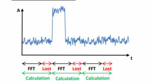
In real-time acquisition the calculation will be performed in parallel to FFT process and the calculation itself is very fast. The calculation is faster than FFT acquisition and contents all operation until displaying the trace to the display. The display data will be changed with very high and constant speed. The result is that time acquisition of different FFT blocks is gap free (see figure 4 below). Speed will be not changed with using of different RBW adjustment.
Gap free FFT example in real-time operation:
Figure 4: FFT in Real-time spectrum analyser without gaps A fixed number of 1024 samples are used for one FFT time acquisition. Each FFT calculation is using a window function. Windowing is important to define a discrete number of time points for calculation. Size of window can be varied and is not fixed in time domain. A variation of window size will have a direct influence of real-time resolution bandwidth [RBW] or the other way around: with changing the RBW, size of window will be changed.
Slew rate, sharp of window and number of window points has an influence to leak effect3, frequency- and amplitude accuracy. Therefore several windows are available in RSA5000 series to use the device for a wide range of applications.
Negative aspect of a filter is, that some signal information will be lost due to amplitude suppression at begin and end of a filter (see figure 5).
Figure 5: unfiltered time signal but with lost amplitude information The position of a time signal like a pulse needs to be in the center of FFT window to transform it correctly into frequency range. In case that a pulse is in between two FFT events, then amplitude is suppressed by filter side loops and is no longer correct (see figure 6).
Figure 6: Amplitude is wrong if signal is located in between of two FFT blocks An overlapping process of FFT events will be used in RSA5000 series to avoid losing signal information. Overlapping has the effect that more spectrums are available over a time period and time resolution is higher. Smaller events can be measured (see figure 7) and signal suppression of single FFT acquisition occurred due windowing is eliminated with overlapping.
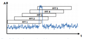
Figure 7: Overlapping process in real-time spectrum analyser In other words, overlapping process of FFT events has a direct influence of smallest pulse width which can be measured with a real-time spectrum analyser. The RT-SA RSA5000 is working with a FFT rate of 146.484 FFT/sec. which results into a calculation speed (Tcalc) of 6,82 µsec.:
Depending on real-time span there are 4 different sample rates available. The maximum sample rate is 51,2 MSa/sec4. With that sample rate and the fixed number of samples (NFix = 1024), used for one FFT acquisition, the duration can be calculated as follow:
An overlap of FFT frames is not possible during calculation progress. Therefore the overlapping time of FFT frames can be calculated with that formula:
𝑇𝑜𝑣𝑒𝑟𝑙𝑎𝑝 = 𝑇𝑎𝑐𝑞 – 𝑇𝑐𝑎𝑙𝑐
For example with sample rate of 51,2 MSa./sec. the overlap time is 13,18 µsec or 65,86% which results into NOverlap = 674 sample points.
Probability of Intercept [POI]
POI specify the smallest pulse duration which can be measured with 100 % amplitude accuracy. Furthermore POI defines the minimum pulse width where each pulse will be captured (see figure 8). The smallest POI of RSA5000 is 7.45 µsec5.
Figure 8: Measurement of a pulse of 7.45 µsec. (period: 1 sec.) with amplitude of -35 dBm. Each pulse is captured with correct amplitude. These small pulse events can’t be measured constantly with a normal SA. A RT-SA is necessary for that kind of short events. RSA5000 can measure a minimum event of 25 nsec., but not with 100% amplitude accuracy and not all pulses will be measured (see figure 9).
Figure 9: Measurement of a pulse of 25 nsec. (period: 1 sec.) with amplitude of -35 dBm. Not all pulses are captured. Amplitude is wrong amplitude. POI depends on FFT rate, used RBW and adjusted Span. The principle of POI is described with a span of 40 MHz (=51,2 MSa/sec.) and RBW of 3.21 MHz (Kaiser Window) in figure 10. Due to calculation time, second FFT acquisition starts after 6.82 µsec. Window size is depending of RBW in real-time mode:
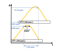
Figure 10: Example with RT-Span of 40 MHz, sample rate of 51.2 MSa/s and RBW of 3.21 MHz (Kaiser Filter) With that POI and speed it is now possible to measure a Bluetooth signal with the RT-SA mode of RSA5000 series. Usage of maximum hold is no longer needed. It is possible to set 6 different RBW settings in RT-SA mode and speed is not affected. RSA5000 provides different measurement modes for the analysis:
- Normal Trace Analysis
- Density Analysis
- Spectrogram
- Power vs Time
In normal mode the trace information of current time is visible. It looks like a trace of a SA but due to the real-time sweep more information is visible at the same time compare to SA. Normal trace analysis is a 2D measurement (power over frequency).
Density Analysis is the same result like normal trace analysis. But with density analysis it is additionally possible to analyse the repetition rate of a signal. Density is working with a colour scheme (from blue = 0% to red = 100%, see figure 8). As more often the signal hits a single pixel point within a certain time, as higher is the percentage which defines the colour of this pixel. For example a constant wave [CW] signal would be visible in red colour. A very short single signal event would be visible in blue colour. The colour percentage can be calculated as follow:
This could be a signal with a pulse width of 30 msec. With acquire time of e.g. 60 msec. n = 50% which would be result into the colour ‘yellow’ (see figure 11, below). The normal trace in density has the colour white. Density analysis is a 3D measurement (power over frequency over repetition rate).
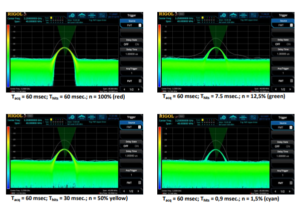
Figure 11: Density example with colour scheme examples In normal and density mode it is possible to activate a spectrogram measurement. Spectrogram is a waterfall measurement frequency over time and bring the possibility to measure out duration of pulses (like for Bluetooth signals). A spectrogram also works with a colour scheme for signal level (DANL: 0% = blue, Reference level: 100% = red). With waterfall spectrogram it is possible to analyse on / off scenarios of signals. Density in combination with spectrogram is a 4D measurement (power over frequency over repetition rate and power over time, see figure 12 with a Bluetooth example).
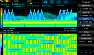
Figure 12: Bluetooth signal measured with density spectrogram In Power vs Time (PvT) it is possible to display the time domain of a signal within adjusted real-time bandwidth. The acquisition time can be changed in this measurement. The Power vs Time analysis is displayed for the used real-time bandwidth and not to RBW like in SA with zero-span configuration. Signal bursts of modulated signals and pulses can be displayed to measure duty cycle and amplitude of a pulse or to display pulse trains over certain time. PvT can be used in combination of normal trace analysis (frequency spectrum) and spectrogram (see figure 13).
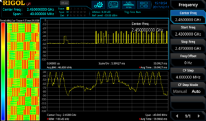
Figure 13: normal trace vs spectrogram vs PvT of a Bluetooth signal Comparing the measurement result of Bluetooth signal in figure 12 and figure 13 and the result of SA (figure 2) test engineer has much more information available now. Within the adjusted real-time bandwidth all frequency components can be measured. Time information can be displayed in parallel of spectrum measurement. In spectrogram it is visible that this signal is a frequency hopping spread spectrum signal and the length of data block can be analysed. The Power vs Time is no longer depended on RBW bandwidth like in SA and frequency domain and time domain can be displayed in one time.
Products Mentioned In This Article:
IoT Antenna Debugging
Wireless Communication and Function
The internet of Things (IoT) is one of the fastest growing areas of technology today. In this increasing competitive field, the greatest challenge facing IoT device manufacturers is determining how to create the smallest devices possible without sacrificing performance in terms of range or power. For IoT devices that utilise radio frequency (RF) communication, one of the greatest opportunities to improve the design of the device while also improving the range and quality; that is, it provides the greatest possible range given the available power and size constraints.
Determining Operating Frequency
To Determine if an antenna is performing as efficiently as possible, the first step is knowing the exact frequency bandwidth that is intended to be used to transmit information. This is generally determined by the communication protocol that will be used, along with the kind of RF circuit that is being designed. This will affect the natural properties of the signal; in general, the higher the frequency the more power is needed to transmit the same information.
Antenna Testing Methodologies
Once the frequency range has been
determined there are several simple tests that can be performed to help identify or verify which antenna will be best suited for the application, including a bandwidth test (or tracking generator test) and a voltage standing waveform ratio (VSWR) test. These two tests will determine the operational bandwidth of a matched set of antennas, and how efficient they are at the desired frequency bandwidth. With a more efficient antenna, less power is required to transmit a signal over a given distance. This can help increased the battery life, reduce the size of the IoT product or add addition range to the product.
Performing a bandwidth test will help to determine if a pair of matched antennas will operate properly at the desired frequency bandwidth. This test must be performed on a spectrum analyser that can operate at the desired frequency bandwidth and has a tracking generator built in; this allows the user to inspect the operating bandwidth as a function of its own power level. This is done by connecting the antenna to the front of a spectrum analyser that has the tracking generator enabled. When the test is performed the spectrum analyser, will transmit a sine wave that is being swept across the desired frequency bandwidth while listening for the signal with the input of the spectrum analyser, and then compare the power level of the transmitted signal. To perform this, test the entire range of the spectrum analyser was used from 9kHz to 7.5GHz to determine the best operating bandwidth for the antennas. See Figure 1.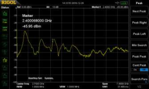
Figure 1: A bandwidth test being performed on two matched antennas that are rated for the 2.4GHz bandwidth. As shown in Figure 1, the frequency ranges where the antenna received the most power at 900MHz bandwidth, 1.5GHz bandwidth and at 2.4GHz bandwidth: therefor this antenna is capable of being used efficiently at these three bandwidths. This makes this antenna and excellent choice for either Wi-Fi or Bluetooth applications which operate at 2.4 GHz bandwidth.
The next test requires the use of a spectrum analyser with a tracking generator as well as a VSWR bridge. The VSWR test is designed to determine the reflection coefficient of a given antenna to help determine the most efficient antenna at a given frequency. VSWR is determined by measuring the voltage standing waves along a transmission line leading to an antenna, it is the ratio of the peak amplitude of a standing wave and the minimum amplitude of a standing wave. When an antenna’s impedance is not matched with the transmission line, power is reflected reducing the amount of transmitted power. The ideal VSWR would be equal to 1 (no power being reflected) at the desired frequency. To perform this, test the desired frequency (2.4GHz) was selected and then the antenna was attached the bridge. A VSWR bridge measures the amount of power that is transmitted into antenna and compares it with the reflect power. Due to the design of a VSWR bridge most of the power that is reflected at a given frequency is the reflected power from the antenna. See Figure 2.
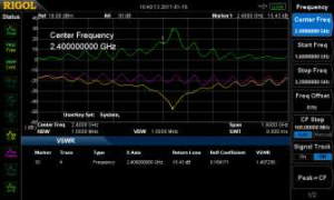
Figure 2: The image shows a VSWR test being performed on an antenna that is meant to operate at 2.4 GHz and has a VSWR of 1.17. Based on Figure 2, the antenna has a VSWR of 1.17 at a frequency of 2.4GHz which makes this antenna almost an ideal antenna for Wi-Fi and Bluetooth communication. With a more efficient antenna, less power is required for transmission, which can increase the effective range of the device. Focusing on improving this one aspect of the IoT device can vastly improve the functionality of the device and address a number of challenges inherent in the overall design.
Additional Areas of Interest
Range is another critical aspect of an IoT device’s design. Sufficient range is required to facilitate wireless communication between IoT devices or with the internet. It is a critical aspect of the initial design and protocol selecting process. For instance, Near-Field Communication (NFC) is a communication technique that is used to transmit information over a couple of inches whereas Bluetooth is used to transmit information for tens of feet. Range requirements will also affect what type of antenna is being used to transmit data, along with determine whether to use a highly directional antenna or an omni directional antenna. Another consideration is the effective range required will determine the amount of power that is needed for transmission; thus, an antenna that makes more efficient use of the available power will help to ensure that the device will have the desired range.Another area of interest to improve the functionality of an IoT device by eliminating or reducing interference to the RF signal. Interference can be generated by the electronic components used in the device itself such as the PCB, battery or user interface, or it can also be generated by the enclosure used to both protect the electronic components and improve the appearance of the device.
Conclusion and Key Learnings
With more Internet of Things devices being conceptualized every day, creating reliable Radio Frequency communication is an essential step towards creating a device that will stand out among the crowd. Successful device manufacturers must overcome the most difficult efficient antenna possible. Key test and measurement equipment will help facilitate basic antenna testing and interference testing that will help overcome these RF communication challenges.FM signal transmission and demodulation demo
Solution: This application note is designed to show FM data transmission and modulation using some common test instruments.
An FM transmission consists of a wave who’s frequency is modulated, or changed, with respect to an input signal. If the input signal frequency changes, so does the carrier frequency.
The modulating signal affects the FM deviation. The total deviation is a function of the modulating signal’s frequency and amplitude.
Here is a typical FM signal shown on an amplitude vs. time graph.
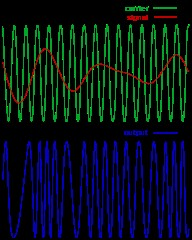
In this demonstration, we are going to use an arbitrary waveform generator to create an FM signal. The FM signal will be modulated by a audio source.
This signal will be transmitted from the output of the generator through an antenna to the input of a spectrum analyser. There, the signal will be displayed on the spectrum analyser, demodulated, and played back through the internal speaker of the instrument.
Required Hardware:
1. A Spectrum Analyser with demodulation capabilities: The Rigol DSA800, 1000, and 1000A series of spectrum analysers all support this function. This demo will use the DSA-1030A, but the process is basically the same.
2. Arbitrary Waveform Generator: Rigol’s DG4000 series is perfect for this experiment. We use the DG4162 160MHz model in this demo.
3. Music source with a headphone jack. In this demo, we will use a cell phone with music source.
4. Adapter cable from music source to BNC cable. In this demo, we made a cable by splicing a 3.5mm audio jack to a 50 ohm coaxial cable with a BNC termination.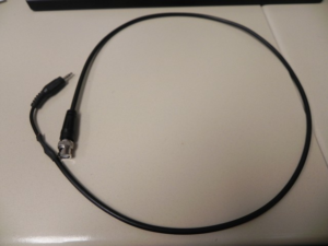
5. N-Type to BNC adapter. This is used to adapt the DSA input to the antenna.
6. Qty 2 FM Radio Antennas with matching frequency ranges. In this demo, we use (2) BNC terminated center loaded whip antennas from Radio Shack.
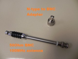
Configure the Arbitrary waveform generator:
In this setup, we want to use the Sine function of the arbitrary waveform to create the carrier wave that supports the signal that we want to transmit and . The audio input signal will be used to modulate the carrier frequency by the deviation that we set.
In the US, commercial radio stations transmit from 87.9 to 107.9MHz. The FM deviation, or amount that the carrier frequency is modulated, is less than or equal to 150kHz, or +/- 75kHz around the carrier frequency.
1. Power on the DG4000.
2. Connect the BNC-to-Phone jack to the CH1 Mod/FSK/TRIG input on the back of the DG4000.
3. Connect the antenna to the Channel 1 output.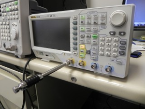
4. Connect your music source and start the music. Make sure to enable the sound on the device.. check that the volume level is > 0.
5. Configure the DG4000 to output a sine by pressing Sine on the Waveform area of the front panel.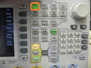
6. Set the frequency of the sine wave to 100.00MHz.

NOTE: You may need to change the frequency by a few 100kHz, if the local radio stations are interfering with the band you are transmitting in. You can simply change the carrier a few 100kHz.
7. Set the amplitude to 2Vpp by pressing the Amp button and then entering 2Vpp on the keypad. Alternately, you can use the scroll wheel to change the values.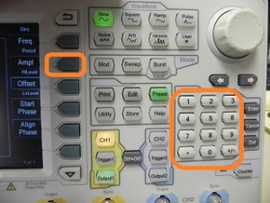
8. Press the Mod key to enable modulation.
• Set type to FM
• Set source to external
• Set deviation to 150kHz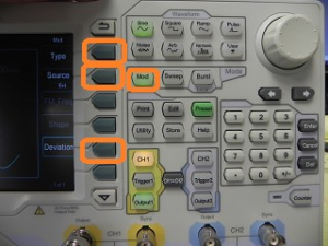
Configure the Spectrum Analyser:
The arbitrary waveform generator is used to create the FM signal and the spectrum analyser is used to capture and demodulate the transmission.
In the US, commercial radio stations transmit from 87.9 to 107.9MHz. The FM deviation, or amount that the carrier frequency is modulated, is less than or equal to 150kHz, or +/- 75kHz around the carrier frequency.
1. Power on the DSA.
2. Connect the N-type adapter and antenna to the RF input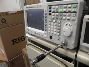
3. BNC-to-Phone jack to the CH1 Mod/FSK/TRIG input on the back of the DG4000.
4. Set the center frequency equal to the carrier frequency of the arbitrary waveform generator. In this example, we have set the DG4000 to output at 100.00MHz.• Press Freq > Center Frequency > 100.00MHz
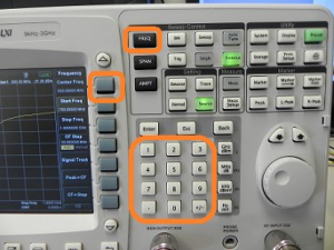
NOTE: You may need to change the frequency by a few 100kHz, if the local radio stations are interfering with the band you are transmitting in. You can simply change the carrier a few 100kHz.
5. Set the span of the DSA to 200kHz.
• Press Span > set span to 200kHz using the keypad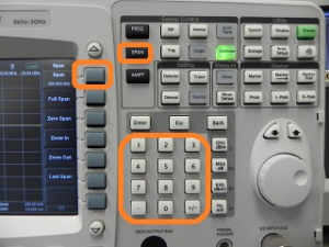
• You should see the signal present on the DSA. You can observe the signal by turning the DG4000 output on and off. The DSA signal should go flat when the DG4000 is off and then rise when the output is on.
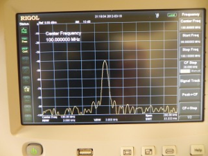
6. Now, we can demodulate the FM signal and listen to the transmission.
• Press Demod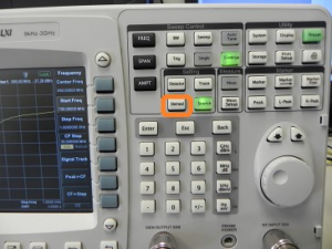
• Enable Demod
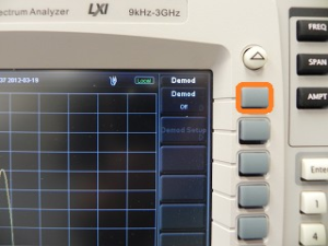
• Press FM
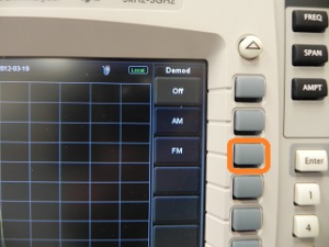
• Press Demod Setup
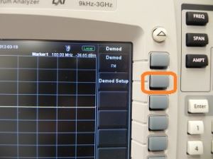
• Turn the Speaker ON
• Set volume to 100
• Set Demo Time to 10s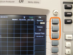
Products Mentioned In This Article:
How to measure a filter using a DSA-815-TG Spectrum Analyser
Solution: This document provides step-by-step instructions on using the Rigol DSA800 series of Spectrum Analysers to measure the characteristics of an RF Bandpass filter.
NOTE: The DSA must have a Tracking Generator to effectively perform the following test.
Normalise the trace (Optional)
Many elements in an RF signal path can have nonlinear characteristics. In many cases, these nonlinear effects on your base measurements can be minimised by normalising the instrument.
1. Connect tracking generator output to RF input using the same cabling that you will be using to test your device. Any element, like an adapter, used during normalisation should also be used during device measurement as any changes to the RF signal path could effect the accuracy of the measurement.
2. Enable the tracking generator by pressing the TG button > TG On
3. Store the reference trace by pressing the TG button > Normalise > Stor Ref
4. Enable normalisation by pressing the TG button > Normalise > Normalise onMeasure the filter
1. Connect the tracking generator output to the filter input using the appropriate cabling and connectors.
2. Connect the filter output to the instrument RF input.
3. Set the tracking generator amplitude by pressing the TG button and the TG Amplitude. You can use the keypad or wheel to enter the correct value.
NOTE: If your instrument is equipped with a Preamplifier, you can enable it to lower the displayed noise floor by pressing the following sequence:
Amplitude button > Down Arrow > RF Preamp On
4. Enable the Tracking generator by pressing the TG button > RF Source ON You can see the small bump in the figure below.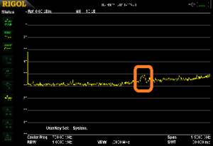
5. You can use the Auto button to center and zoom on the waveform. You can also use the Freq and Span buttons to manually manipulate the displayed data.
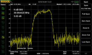
6. You can now enable the Marker function to measure the bandwidth and attenuation or passband characteristics of the filter.
7. Press Marker Fctn > N dB BW and set the function to the amplitude of interest. In this example, we are measuring the 3dB Bandwidth of our filter.
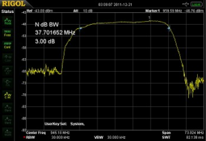
Products Mentioned In This Article:
- DSA800 Series please see HERE