Your cart is currently empty!
Author: James

Programming Example: Performing a series of measurements with an SDM and Scan Card
Here are a list of recommended commands for programmatically executing a scan with a SIGLENT SDM3055 or SDM3065X with scan card option (formerly the SC1016 option)
NOTE: # indicates a comment. You may need to change this symbol, depending on which programming environment you choose to use.
The commands, shown in quotes, will need to be sent using the appropriate function call for the program environment and command type. More information on each command can be found in the Programming Guide for the SDM. For exact command syntax, please refer to your programming environment documentation.
“ROUT:SCAN ON” #Enable scan
“ROUT:FUNC STEP” #Select step type of scan
“ROUT:DCV:AZ OFF” #Turn off the Autozero. Scan will execute more quickly, but accuracy may suffer over time due to drift
“ROUT:CHAN 1,ON,DCV,AUTO,FAST” #Configure Channel 1
“ROUT:CHAN 2,ON,DCV,AUTO,FAST” #Configure Channel 2
“ROUT:CHAN 3,ON,DCV,AUTO,FAST” #Configure Channel 3
“ROUT:CHAN 4,ON,DCV,AUTO,FAST” #Configure Channel 4
“ROUT:CHAN 5,ON,DCV,AUTO,FAST” #Configure Channel 5
#The scan will start at the Low channel and step to the High, defined below
“ROUT:LIMI:HIGH 5” #This sets the highest channel value in the scan list
“ROUT:LIMI:LOW 1” #This sets the lowest channel value in the scan list
“ROUTe:COUN 1” #Perform a single scan
“ROUTe:START ON” #Begin scan
#Poll (loop, when response matches “OFF”, scan is finished)
“ROUT:START?” #Is the scan finished?
#Insert proper READ statement here to evaluate return string for poll
#Return data string from each channel individually
“ROUT:DATA? 1”
#Insert proper READ statement here to return the data string
“ROUT:DATA? 2”
#Insert proper READ statement here to return the data string
“ROUTe:DATA? 3”
#Insert proper READ statement here to return the data string
“ROUTe:DATA? 4”
#Insert proper READ statement here to return the data string
“ROUTe:DATA? 5”
#Insert proper READ statement here to return the data string

Measuring Power Supply Control Loop Response with Bode Plot II
Stability is one of the most important characteristics in power supply design. Traditionally, stability measurements require expensive frequency response analyzers (FRA) which are not always available in a laboratory. Now, using a Siglent oscilloscope, like the SDS1204X-E with the newly released Bode Plot Ⅱ software, together with a Siglent arbitrary waveform generator (SDG or SAG) and a Picotest injection transformer, the measurement can be made.
In this application note, we will show you the basic principles for making this stability measurement and how to use these instruments to make the measurement.
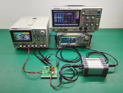 Figure 1: Bode II setup
1. Basic Principle of Stability Measurement
1.1 Stability of The Feedback System
A regulated power supply is actually a feedback amplifier with a large amount of current sourcing capability. Any theory that applies to a basic feedback amplifier also applies to a regulated power supply.
In feedback theory, the stability of a feedback system can be determined by evaluating the loop transfer function. A more practical way is to measure the bode plot of the loop gain. Figure 2 shows a typical feedback system.
The closed loop transfer A is the mathematical relationship between input x and output y. The loop gain T, by its name, is defined as the gain of a signal traveling around the loop.
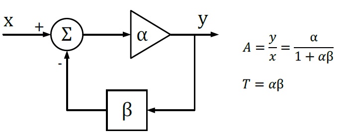 Figure 2: Typical Feedback Loop
Since α and β are complex variables, they have not only magnitude but also phase angle, as also does the loop gain T. If the phase angle of T reaches -180° while the magnitude is 1, the closed-loop transfer function A becomes infinity. In this situation, the system will maintain an output signal while there is no input. Thus, the system acts as an oscillator rather than as an amplifier, which means that the system is not stable.
If we plot the loop gain in a bode plot, we can evaluate the stability by finding the phase margin and gain margin. A phase margin is defined as how many degrees the phase can be decreased before reaching -180°while the magnitude is 1 (or 0 dB). The gain margin is defined as how many dB in magnitude can be added before reaching 1 (or 0 dB) while the phase is -180°.
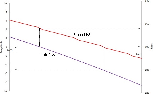 Figure 3: Bode Plot, phase, and gain margin
1.2 Break the Loop
To get the desired loop gain, we simply break the loop. Figure 4 shows how to break the loop in a typical feedback system. Technically you can break the loop any place you like. We commonly choose to break the loop at the point between the amplifier output and the feedback network. Then we insert a test signal i to travel around the loop. The loop gain is the mathematical relationship between the output y and the test signal i.
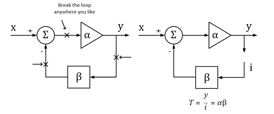 Figure 4: Breaking the loop in a typical feedback system
1.3 Loop Injection
In reality, we can never really break the loop because the feedback loop serves to maintain the DC quiescent operation point of the circuits. Without the feedback loop, the device under test will become saturated because of the small input offset voltage, and then no useful result can be measured.
To overcome this, we should measure the open loop response inside a closed loop. Therefore, we just inject a signal to the loop rather than breaking the loop. Figure 5 shows a typical method of loop injection. The injection point is chosen so that the impedance looking in the direction of the loop is much higher than that looking backward. One possible point is between the output and the resistor divider feedback network. Other points that meet this requirement may be chosen.
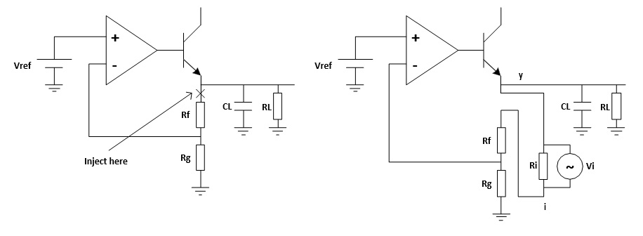 Figure 5: Loop injection
To maintain the closed loop, a small injection resistor Ri is inserted at the injection point. The resistor should be small enough so that it will have little effect on the circuit and also the lower the resistor value the lower the frequency the transformer will operate. Picotest recommends a resistor value of 4.99 Ω for the J2100A, and larger value may be chosen depending on the circuits. The injection signal is then applied across the injection resistor.
The signal injected should have no effect on the DC operating point of the circuit. A method to solve the common ground connection problem is to use an injection transformer as shown in Figure 6.
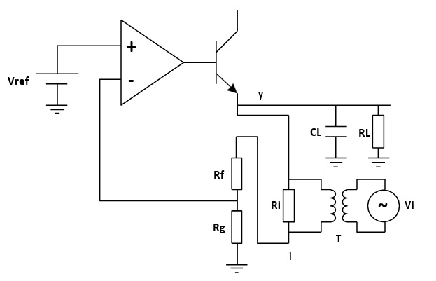 Figure 6: Injection Transformer
The injection signal starts at one end of the injection resistor, travels through the resistor divider feedback network, the error amplifier and the pass element transistor and finally to the output, which is the other end of the injection resistor. The relationship between the injection signal i and the output signal y is the loop gain that we wish to measure.
Be aware that we are measuring an open loop parameter inside a closed loop, the phase starts at 180°and decreases to 0°, rather than starting at 0°and decreasing to -180°. So the phase margin should be measured relative to 0°.
2. Measurement Setup and Result
2.1 Equipment
Oscilloscope: Siglent SDS1204X-E with firmware version higher than 6.1.27R1 (Bode Plot Ⅱ release)
Signal Source: Siglent SDG2042X
Power Supply: Siglent SPD3303X
Probe: Siglent PP215 passive probe switched to 1X
Injection Transformer: Picotest J2100A
Device-Under-Test: Picotest VRTS v1.51
2.2 Circuit Connection
The Picotest VRTS v1.51 is a demonstration board for voltage regulator testing. Technically it is a linear regulator built from the famous TL431 and a discrete transistor. The schematic is shown in Figure 7. Different output capacitors can be selected to see the impact on the control loop stability.
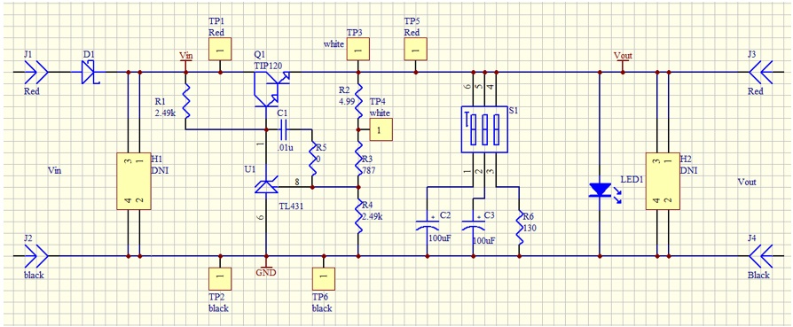 Figure 7: VRTS v1.51 schematic
For the propose of our power supply control loop response measurement, the injection point is TP3 and TP4. The circuit connection is shown in Figure 8.
The generator is connected to the oscilloscope through USB (connection through Ethernet is also supported).
The injection transformer is connected in parallel with the injection resistor so that the signal is injected to the loop while preventing the circuit DC operation point from being affected by the generator.
The TP3 and TP4 points are also connected to the oscilloscope, and the TP4 is defined as the DUT Input while the TP3 is the DUT Output in the Bode Plot Ⅱ.
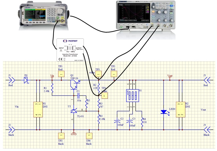 Figure 8: Circuit connection
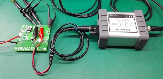 Figure 9: Probe and Transformer connections to the DUT
2.3 Instrument Configuration
In this section, we will show how the key configuration should be made in order to make the measurement correctly. For complete instructions to the Bode Plot Ⅱ, please refer to the user manual and the quick start guide.
Before entering the Bode Plot Ⅱ, it is recommended that you enable the oscilloscope’s 20 MHz bandwidth limit setting.
At this time, we want to measure the bode plot from 10 Hz all the way to 100 kHz. This frequency range should be enough for a circuit with an expected crossover frequency at about 10 kHz.
Enter the Config menu and set the Sweep Type to Simple, then enter Set Sweep to set the sweeping frequency. Set the Mode to Decade and Start to 10 Hz, Stop to 100 kHz. Set Points/dec to 20, enough for a typical sweep. Enter the Set Stimulus menu to set Amplitude to 50 mV. Enter the Set Channel menu to set DUT Input to CH1 and DUT Output to CH2.
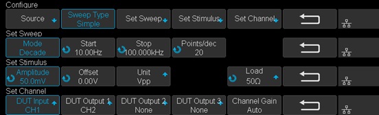 Figure 10: Bode II scope configuration
2.4 Results and Data analysis
After the configuration is done, return to the main menu and press Run to start the sweep.
Wait to see the results as shown in Figure 11.
The result is somewhat confusing and suspect because of the trace at low frequency, especially the phase trace, alternating up and down. We will introduce a method called Vari-level to resolve this problem in the next section.
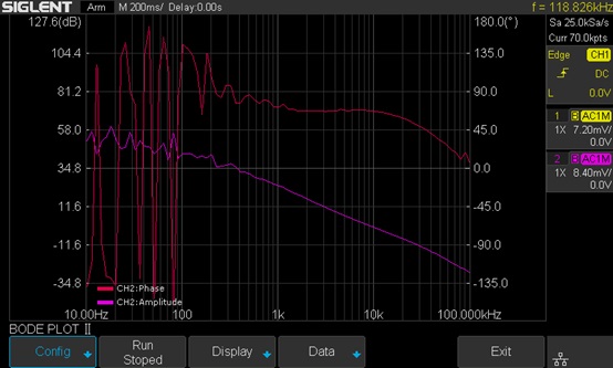 Figure 11: Measurement results
After the sweep has completed, press Run again to stop the sweep. Enter the Display menu and then enter the Cursors menu to turn on the cursors. Use the Adjust knob to move the cursors and set the phase margin as shown in Figure 12.
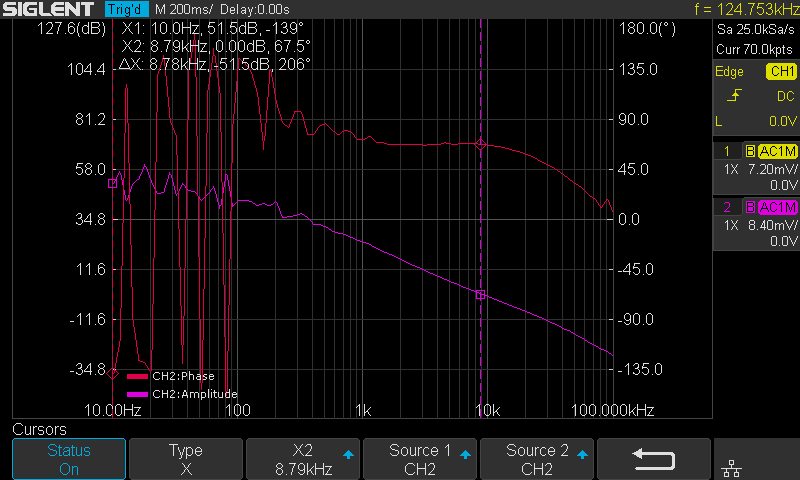 Figure 12: Cursor measurement on the Bode plot
You can also turn on the List feature in the Data menu to examine the measured data, or you can export the data to an external USB FLASH driver for further analysis on a computer.
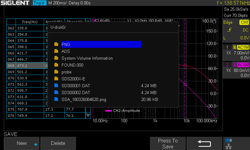 Figure 13: Exporting data
2.5 Vari-level
In the previous section, we can see that the results are not ideal, for the bouncing trace at low frequency. This is because at low frequency the amplitude difference between the input and output channel is relatively large, and since we are using a relatively small stimulus signal (this time 50 mVpp), the signal presented at the DUT Input channel is extremely small so that a commercial general propose oscilloscope cannot measure it accurately.
But we cannot simply increase the stimulus’ signal amplitude. The result will be similar to what is shown in Figure 14. The large signal near the crossover frequency region causes serious distortion to the loop. The distorted signal in the time domain is shown in Figure 15.
Remember that a bode plot only makes sense in a linear system, and has no meaning in a heavily non-linear system. The result is useless.
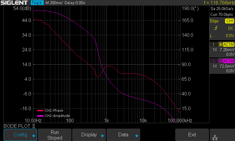 Figure 14: Increased stimulus signal amplitude and distortion
 Figure 15: Distortion in the time domain
One possible solution to the problem is Vari-level (other manufactures may call it “Shaped Level” or “Level Profile”). The Vari-level concept is simple: The stimulus signal amplitude is variable over the frequency. If we use a large signal at low frequencies, and decrease the amplitude to a fairly small level near the crossover region so that it causes little distortion to the loop, in theory, we can get an ideal result.
Under the Configure menu, set Sweep Type from Simple to Vari-level, and push Set Vari-level to enter the Vari-level profile editor.
 Figure 16: Set Sweep Type to Vari-level
Figure 17 shows the Vari-level profile editor. The Profile option allows the user to select and save up to 4 profiles. The Nodes sets the number of nodes in the profile trace, the minimum allowed number of nodes is 2 because at least 2 points can determine a line, and always the first and the last node set the start and stop of the trace. Press Edit Table will enter the profile editor mode. The parameter under editing is highlighted by cursors, and next push Edit Table again to cycle the cursors between “Freq”, “Ampl” and the entire row, which allows the user to navigate through the entire table. Users can use the Adjust knob to set the highlighted parameter, and pushing the knob will call out a visual keypad which allows direct input to the parameter. The Set Sweep and Set Stimulus option is somewhat similar to that in the Simple type of sweep, but they are not correlated. This time we set the sweep Mode to Decade and a 40-point-per-decade is sufficient. The profile shown in Figure 17 is used in this measurement. It is not the optimum profile for this circuit but should be a good place to start.
 Figure 17: Vari-level profile editor
In practice, one should always experiment with those parameters to find an optimum solution for a particular circuit.
One practical way to do this is to monitor the signal in the time domain, decrease the amplitude of the stimulus signal until no visible distortion can be observed, then decrease the amplitude by another 6 dB. Next, record the amplitude and frequency, jump to another frequency and repeat the process.
There is a better way to find the optimum profile if you already have a known good profile. Reduce the signal amplitude by 6 dB and run a sweep to see if the plot changes. If it does change, reduce the amplitude by another 6 dB and sweep again. Until the result doesn’t change, then you can increase the amplitude by 6 dB and that’s an optimum profile. This is time-consuming but necessary to get a meaningful result.
Once profile editing is completed, return to the main menu and push Run to start the sweep. Figure 18 shows the final result of the measurement with Vari-level. Changing the capacitor selection switch S1 on the VRTS v1.51 demo board will alter the loop response due to the impact of different capacitors.
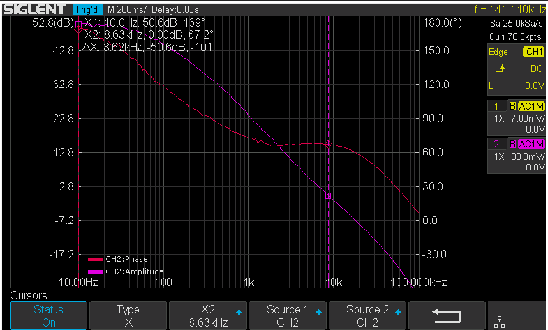 Figure 18: Results with Vari-level
3. Summary
The Siglent oscilloscope with newly released Bode Plot Ⅱ together with a Siglent signal generator and a Picotest injection transformer offer a very flexible and easy-to-use power supply control loop measurement system.
Quick remote computer control using LXI Tools
Introduction:
There are many options for people considering remote communication and control of test and measurement instrumentation. In most cases, a computer is used to communicate to test instrumentation using USB or LAN connections. The computer can configure the instruments, collect and organize data, and present it in a useful and flexible way.
Remote control provides:
- Increased repeatability: The instrumentation is set up the same way, every time.
- Efficient data collection: Data can be automatically filtered and stored.
- Easily configure the test system parameters: Each command is executed in the same order and in the same timeframe.
- Quickly visualize system performance: Graphical or tabular data formatting is easy.
There are numerous platforms (Windows, Linux, etc..) and software programs (LabVIEW, .NET, Python) available to build automated test systems. The right choice for your application is highly dependent on your needs and the available skills you have.
In this note, we are going to discuss how to use LXI Tools to communicate with SIGLENT instrumentation. LXI Tools is an open source software application that uses the local area network (LAN) connection to quickly control remote instrumentation. It is easy to install, has a small operating footprint, and is really powerful while being quite easy to use. Let’s start by looking at the basics.
You can also see the video version of this note here: https://siglentna.com/video/lxi-tools/
Why Open Source?
Open source coding is a community-based development style in which a group of contributors work together to build and maintain programs using shared code and components. In this way, a platform can be built and tested quickly and may cost significantly less than commercial programming environments. LXI Tools is free open source software and the project welcomes new contributors that would like to help improve the tools.
Here is a link to the LXI Tools website: https://lxi-tools.github.io
Why LXI Tools?
LXI-Tools is a collection of open source software tools that provide direct control of LXI compatible instruments such as modern oscilloscopes, power supplies, spectrum analyzers, and more.Simply install LXI Tools, connect your instrument, and start communicating.
It really is that easy.
LXI-Tools Provides:
- Quickly discover the available instruments on the LAN
- Retrieve copies of the displayed images (quickly see signals, data, and instrumentation setups) and convert image file types
- Benchmark LAN performance
- Send individual commands to an instrument to perform simple test actions. For example, you could return the measured data from a DMM.
To learn more about LXI-Tools, please see https://github.com/lxi-tools/lxi-tools
Instructions:
- Install the appropriate version of LXI-Tools for your operating system
2. Open a terminal. In this example, I am using Ubuntu (17.10) running on a virtual machine hosted by a Win 10/64 bit OS.
To learn more about the virtual machine used in this example:https://www.virtualbox.org/
The OS is Ubuntu: https://www.ubuntu.com/
3. Once loaded, startup Linux:
With Ubuntu, you can use Snap to install:
$ snap install lxi-tools
LXI Discover:
Quickly searches the LAN for instruments and lists their identification string and IP address.
Plug in and power on your instrumentation and make sure that they are connected to a working LAN connection. You can manually check the instrument IP address and save this info to compare to later steps.
Open up a terminal window. At the “$” prompt, simply type lxi discover… LXI tools will search the LAN for connected instruments.
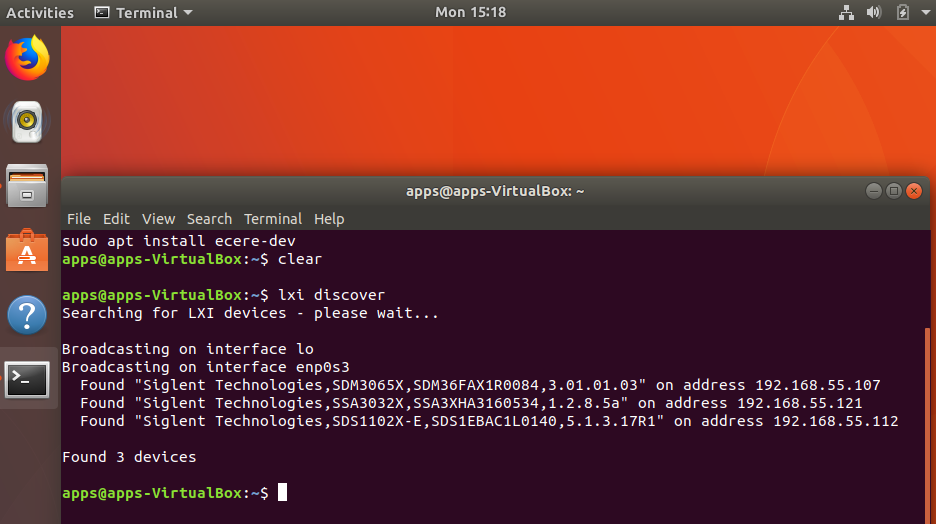
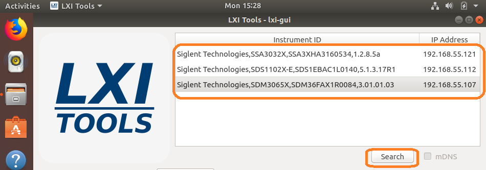
Here, we have three devices connected: an SDM3065X, SSA3032X, and an SDS1102X-E (which has been superseded by the SDS1202X-E series here in North America). It also includes the instrument serial number, firmware revision, and IP address.
NOTE: This has been tested with a large number of instruments, but may not be supported by some. There is a list of compatible instruments at the end of this note or you can check LXI-Tools support for the latest list of supported products.
Screenshot:
This function retrieves a copy of the instrument display and saves it to the local drive. This is ideal for adding information to reports and sharing events with colleagues.
Type “lxi screenshot – – address <device address>”
NOTE: There should be two “-” with no spaces before “address” for every command.

Image Edits using ImageMagicks
Use ImageMagick® to create, edit, compose, or convert bitmap images. It can read and write images in a variety of formats (over 200) including PNG, JPEG, JPEG-2000, GIF, TIFF, DPX, EXR, WebP, Postscript, PDF, and SVG. Use ImageMagick to resize, flip, mirror, rotate, distort, shear and transform images, adjust image colors, apply various special effects, or draw text, lines, polygons, ellipses and Bézier curves.
For more information, visit… https://www.imagemagick.org/script/index.php
$ lxi screenshot –address <ip> – | convert – screenshot.jpg
$ lxi screenshot –address <ip> – | convert – screenshot.tiff
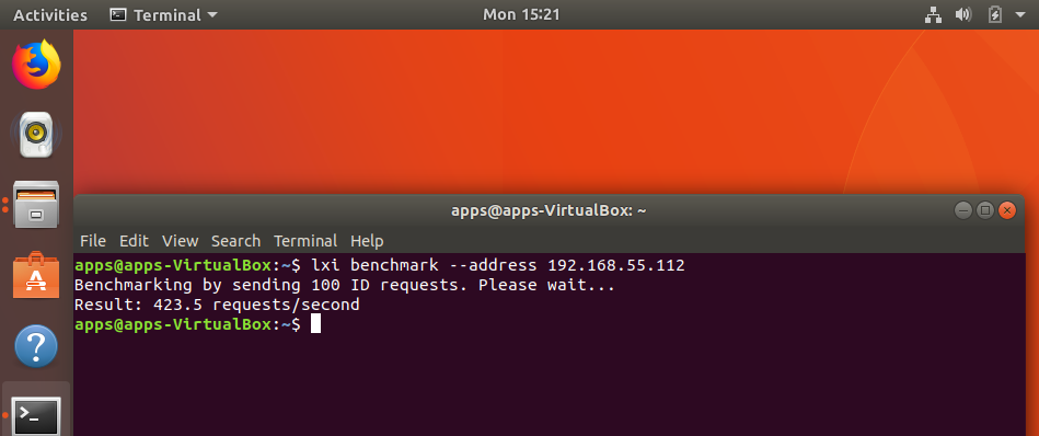
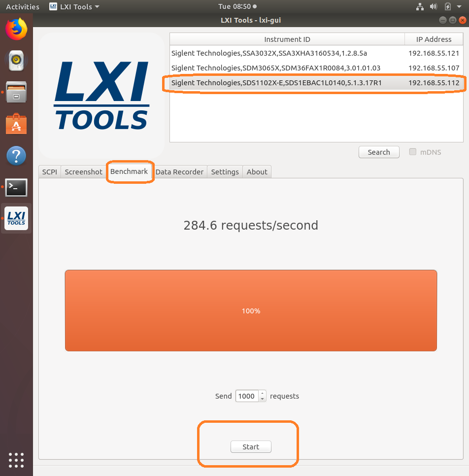
$ lxi screenshot –address <ip> – | convert – screenshot.bmpBenchmark:
The benchmark command sends 100 requests via LAN and measures the average response time of the instrument. It can be used as a gauge for the health of the connection. Higher response rates = faster links.
$ lxi benchmark –address <ip>
Manual vs. Auto-load:
The commands can also be manually or auto-loaded:
Auto-load/detect:
$ lxi screenshot –address 10.0.0.42
Vs. manually specifying which screenshot plugin to use:
$ lxi screenshot –address 10.0.0.42 –plugin siglent-ssa3000x
The only advantage of manually specifying which plugin to use it that it is a bit faster because it does not go through the instrument auto detection steps (retrieve ID, parse regex rules to match correct plugin etc.).
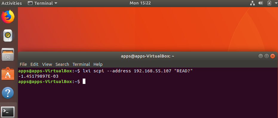
Sending instrument specific commands:
You can also use the SCPI command to send any command to the instrument.
Note that if you have an SCPI command with spaces you must remember to send the specific command in quotes like so:
$ lxi scpi –address 192.168.55.113 “MEAS:VOLT? CH1”
This way the tool knows how to parse the full SCPI string.
In this example, we send the “READ?” command to an SDM and return a reading:
GUI
Another really great feature is the GUI for LXI Tools. This allows you easy access to discovery of instruments on the network as well as some powerful tools for data capture and instrument control.
$ lxi-tools.lxi-gui
This adds a very simple yet powerful graphical interface for the LXI tools program:
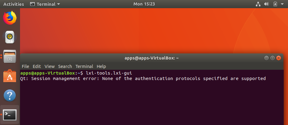
NOTE: Ignore the “Qt” error shown.
This opens a clean control window:
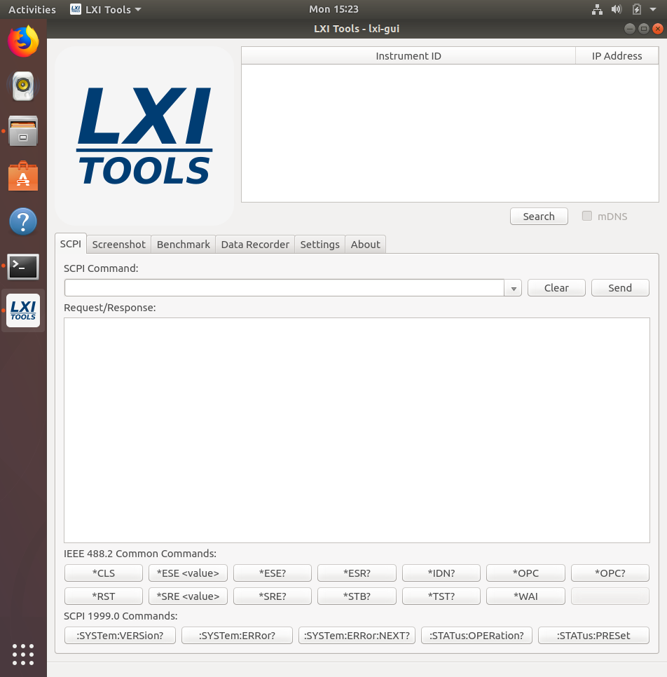
- Search: Discover the instruments connected to the LAN. Here, we have three instruments connected:
- SCPI command line: Send instrument specific commands. Click on the instrument you wish to communicate with and then enter the command. For queries (commands that require an instrument response, or read function), the returned string will be shown in the text box:
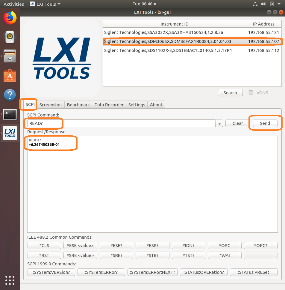
NOTE: The specific commands that can be used are available in the instrument programming guide. Check out the specific instrument documentation for more details.
This tool can be helpful when trying out specific sequences of commands. You can send them one-at-a-time and then observe the instrument functionality.
- Screenshot: Capture and save an image from the instrument. This also features a “live” button that will continuously poll the instrument.
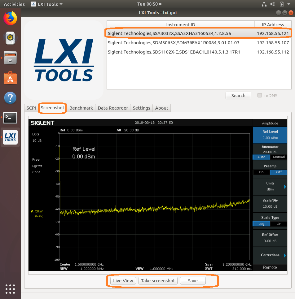
After saving, you can recall the image:
- Benchmark: Checks the performance of the LAN connection by sending a series of commands and measuring the response time. Larger “requests/second” = greater possible bus performance.
- Data Recorder: Sends the user-defined command a number of times/second and attempts to graph the data. Be aware that data can be returned in different formats and at different rates depending on device configuration. Going faster can make the system unstable and could cause a crash or hang-up.
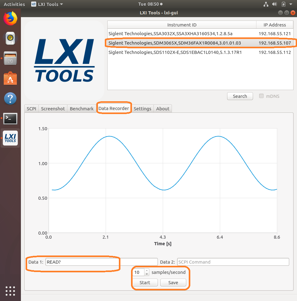
And the data:

- Settings: Configure the timeouts and other controls.

- About: Version info.
*Here is a list of the latest compatible instruments tested with Lxi-Tools (03/13/2018)
SSA3000X Series:
SSA3000X (Latest 1.2.8.5a)
SDS1000X-E Series:
SDS1202X-E (Older 5.1.3.8R2)
SDS1202X-E (Latest 5.1.3.13)
SDS1204X-E (Latest/first production release 7.6.1.12)
SDS1000X/X+ Series:
SDS1202X+ (Latest 1.1.2.15E3)*
*LIMITED COMMAND SET AVAILABILITY
SDS2000X Series:
SDS2304X (Older 1.2.2.2)*
SDS2304X (Latest 1.2.2.2R10)*
*LIMITED COMMAND SET AVAILABILITY
SDS2000 Series (replaced by the SDS2000X):
SDS2204 (Latest 1.2.2.2)*
*LIMITED COMMAND SET AVAILABILITY
SDM3000 Series:
SDM3045X (Older rev 5.01.01.01)
SDM3045X (Latest rev 5.01.01.03)
SDM3055 (Latest rev 1.01.01.01.19)
SDM3065X (Older rev 3.01.01.02)
SDM3065X (Latest rev 3.01.01.03)
SDG1/2/6X Series:
SDG1032X (Latest 1.01.01.22R5)
SDG20122X (2.01.01.23R7)
SDG6052X (Latest 6.01.01.28R1): 405.3

Programming Example: Using Python to configure a basic waveform with an SDG X series generator via o
#!/usr/bin/env python 2.7.13
#-*- coding:utf-8 –*-
#—————————————————————————–
# The short script is a example that open a socket, sends basic commands
# to set the waveform type, amplitude, and frequency and closes the socket.
#
#No warranties expressed or implied
#
#SIGLENT/JAC 11.2018
#
#—————————————————————————–
import socket # for sockets
import sys # for exit
import time # for sleep
#—————————————————————————–remote_ip = “192.168.55.110” # should match the instrument’s IP address
port = 5024 # the port number of the instrument service#Port 5024 is valid for the following:
#SIGLENT SDS1202X-E, SDG2X Series, SDG6X Series
#SDM3055, SDM3045X, and SDM3065X
#
#Port 5025 is valid for the following:
#SIGLENT SVA1000X series, SSA3000X Series, and SPD3303X/XEcount = 0
def SocketConnect():
try:
#create an AF_INET, STREAM socket (TCP)
s = socket.socket(socket.AF_INET, socket.SOCK_STREAM)
except socket.error:
print (‘Failed to create socket.’)
sys.exit();
try:
#Connect to remote server
s.connect((remote_ip , port))
except socket.error:
print (‘failed to connect to ip ‘ + remote_ip)
return sdef SocketSend(Sock, cmd):
try :
#Send cmd string
Sock.sendall(cmd)
Sock.sendall(b’\n’)
time.sleep(1)
except socket.error:
#Send failed
print (‘Send failed’)
sys.exit()
#reply = Sock.recv(4096)
#return replydef SocketClose(Sock):
#close the socket
Sock.close()
time.sleep(1)def main():
global remote_ip
global port
global count# Body: send the SCPI commands and print the return message
s = SocketConnect()
qStr = SocketSend(s, b’*RST’) #Reset to factory defaults
time.sleep(1)qStr = SocketSend(s, b’C1:BSWV WVTP,SQUARE’) #Set CH1 Wavetype to Square
qStr = SocketSend(s, b’C1:BSWV FRQ,1000′) #Set CH1 Frequency
qStr = SocketSend(s, b’C1:BSWV AMP,1′) #Set CH1 amplitudeSocketClose(s) #Close socket
print(‘Query complete. Exiting program’)
sys.exitif __name__ == ‘__main__’:
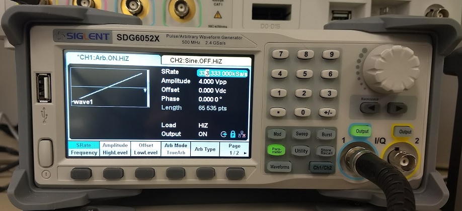
proc = main()Python Example: Building an Arb with 16-bit steps (SDG2000X/SDG6000X)
The SIGLENT SDG2000X and SDG6000X feature 16-bit voltage step resolution. This provides 65,535 discrete voltage steps that can cover the entire output range (20 Vpp into a High Z load) which can effectively be used to test A/D converters and other measurement systems by sourcing waveforms with very small changes.
In this example, we use Python 2.7 and PyVISA 1.8 to create a ramp waveform that is comprised of steps of the Least Significant Bit (LSB) from point 0 to 65535 on Channel 1.
We also implement the TrueArb function that allows you to specify the sample rate and also ensures that each sample is sourced.
NOTE: You will need to change the instrument ID to match your specific instrument. We also recommend setting the amplitude and other instrument parameters prior to enabling the output of the instrument.
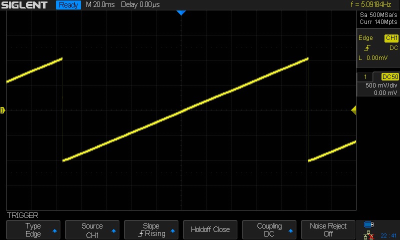
Here is pic of the instrument after loading the waveform:
Here is a scope shot of the output:
Here is a link to a Zipped version of the .PY file: SiglentSDG16BBitSteps
Here is the text of the program:
##
#!/usr/bin/env python2.7
# -*- coding: utf-8 -*-
import visa #Uses PyVISA 1.8 and NI-VISA runtime Engine 15.5
import time
import binascii#USB resource of Device
rm = visa.ResourceManager()
device = rm.open_resource(‘USB0::0xF4EC::0x1101::SDG6XBAQ1R0071::INSTR’) #CHANGE TO MATCH YOUR INSTRUMENT ID#Little endian, 16-bit 2’s complement
# create a waveformwave_points = []
for pt in range(0x8000, 0xffff, 1):
wave_points.append(pt)
wave_points.append(0xffff)
for pt in range(0x0000, 0x7fff, 1):
wave_points.append(pt)def create_wave_file():
#create a file
f = open(“wave1.bin”, “wb”)
for a in wave_points:
b = hex(a)
#print ‘wave_points: ‘,a,b
b = b[2:]
len_b = len(b)
if (0 == len_b):
b = ‘0000’
elif (1 == len_b):
b = ‘000’ + b
elif (2 == len_b):
b = ’00’ + b
elif (3 == len_b):
b = ‘0’ + b
b = b[2:4] + b[:2] #change big-endian to little-endian
c = binascii.a2b_hex(b) #Hexadecimal integer to ASCii encoded string
f.write(c)
f.close()def send_wave_data(dev):
#send wave1.bin to the device
f = open(“wave1.bin”, “rb”) #wave1.bin is the waveform to be sent
data = f.read()
print (“write bytes:”,len(data))
dev.write_raw(“C1:WVDT WVNM,wave1,FREQ,2000.0,TYPE,8,AMPL,4.0,OFST,0.0,PHASE,0.0,WAVEDATA,%s” % (data))
#”X” series (SDG1000X/SDG2000X/SDG6000X/X-E)
dev.write(“C1:ARWV NAME,wave1”)
f.close()if __name__ == ‘__main__’:
create_wave_file()
send_wave_data(device)
device.write(“C1:SRATE MODE,TARB,VALUE,333333,INTER,LINE”) #Use TrueArb and fixed sample rate to play every point###
Resolver Simulation using an Arbitrary Waveform Generator
A resolver is an electromagnetic sensor that is used to determine the mechanical angle and velocity of a shaft or axle. They are often used in automotive applications (cam/crankshaft position), aeronautics (flap position), as well as servos and industrial applications.
When designing, testing, or troubleshooting systems that use resolvers, it can be worthwhile to build a system that can easy simulate the output of a resolver. This is especially helpful when testing the operational limits of the resolver measurement circuitry and any code that may accompany these measurements. Simulation allows you to control and test the limits of operation of a system by adding known errors to the signal or by changing the frequency/amplitude/waveform shapes to see where the system begins to fail.
In this application note, we are going to describe a method of simulating a simple resolver using a SIGLENT SDG2000X Series arbitrary waveform generator.
RESOLVER BASICS
Many resolvers share a similar design as shown in Figure 1: A primary winding or coil that is attached to a shaft or rotor, and two stationary windings, or stators that are positioned at 90 degrees to one another.
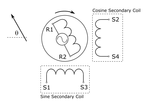
Figure 1: Basic resolver design.The primary winding is energized with an AC Voltage, Vr. This primary excitation signal is typically a sinewave that is then coupled into both secondary coils. In many resolvers, the secondary coils are built such that coils are physically mounted 90 degrees from one another. Since each coil is physically located in a different location with respect to the primary coil, they will each have different coupling efficiency and, because they are mounted 90 degrees apart, their outputs will be orthogonal (90 degrees out-of-phase of each other). As the shaft angle changes, the output signal for the secondary coils will change as shown in Figure 2.
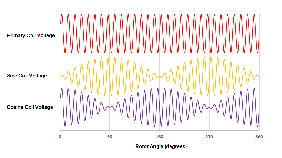
Figure 2: Coil voltage vs Rotor Angle for a sine primary voltage.Therefore, there are discrete voltage values for each shaft angle. By measuring the instantaneous voltages of the secondary coils, you can determine the rotor angle.
EQUIPMENT
In this simulation, we are going to use a waveform generator to source the primary coil signal. This signal will be used to simultaneously modulate the outputs of a dual channel generator. These outputs will represent the secondary sine and cosine coil output signals, as discussed previously.
- SDG805: Modulation source for secondary coil outputs.This instrument should be able to match the primary coil minimum and maximum frequency specifications of the resolver you are simulating. Many resolvers have primary coil signals that vary from 5 k to 20 kHz and a few hundred mV to 100’s of volts. These higher voltages are used to excite the secondary coils.
- SDG1032X: Secondary coil simulation.This model has a single external modulation input, independent phase control, and Dual Side Band AM (DSB-AM) modulation which we will need to successfully simulate the sine and cosine signals of a resolver.
- Dual Channel Oscilloscope: Signal verification.It is important to select a scope with the proper bandwidth (at least 2 to 3x the max frequency of primary frequency, even higher if the primary has higher harmonics/square wave). In this example, we are going to use a SIGLENT SDS2102X. This platform has deep memory (140M points), zoom, and a large display that will make verification easier.
SETUP
Use a BNC terminated cable to connect CH1 output of the primary generator to the Aux/Mod In of the secondary coil generator, as shown below in Figure 3.
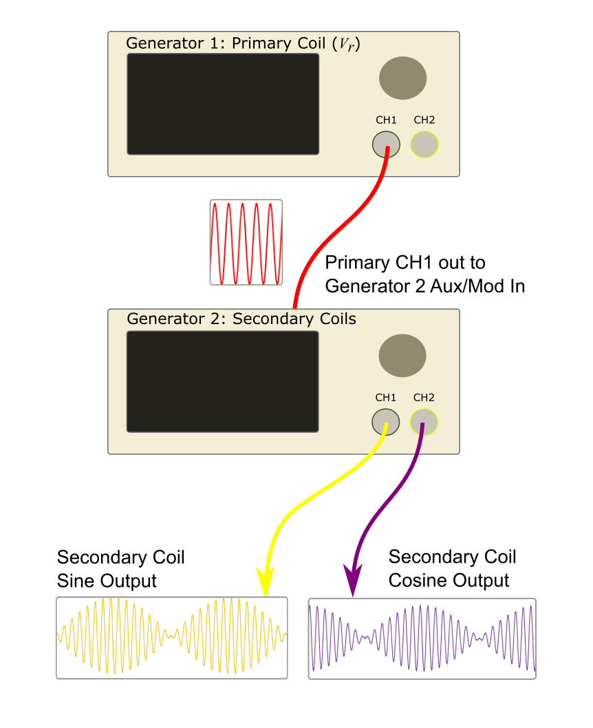
Figure 3: Physical connections between the two generators.1. Connect the secondary coil outputs of the second generator (CH1 and CH2) to the inputs of the oscilloscope.
2. Configure the primary coil generator to output a sine wave at the lowest frequency of Vr for your system. Typically, the Vr frequency ranges from 5 k to 20 kHz.
The primary coil generator is going to be used to modulate the output signals of the secondary coil generator. The voltage for the primary signal should be low to start (5Vpp). We will optimize it later.
3. Set the secondary coil generator CH1 to output a sine wave with a frequency of 1Hz, voltage of 10Vpp (or equivalent to the maximum voltage of your resolver circuit).
4. Set the secondary coil generator CH1 to perform a Dual-Side-Band AM (DSB AM) modulation by pressing Mod and select the DSB-AM type.
5. Configure CH2 on the secondary coil generator to output the same modulated sine signal as channel 1, only set the phase offset to 90 degrees. This will provide the orthogonal output phase for the secondary cosine channel.
The secondary coil frequency represents the rotational frequency of the rotating primary coil in a physical resolver. Be sure to set both CH1 and CH2 to the same frequency.
NOTE: The SIGLENT SDG1000X and SDS2000X series feature a Channel Copy
And a channel coupling function which makes the process easier.To couple the frequency selection between two channels, press Utility > CH Copy Coupling > FreqCoupl = ON. Now, any changes in frequency on either channel will be applied to the other channel. This allows you to simultaneously change both frequencies.
To copy settings from one channel to another, press Utility > CH Copy Coupling > CH Copy > CH1 => CH2
6. Enable the primary coil generator CH1 and both outputs of the secondary coil generator.
7. Verify the performance, adjust the secondary coil frequency (rate of change of the rotor), verify, and so on until you have fully tested the limits of the resolver system.
The figures below show images of secondary coil simulations at various primary coil frequencies and secondary coil frequencies:
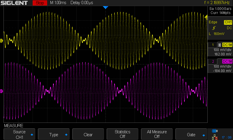
Figure 4: Primary coil 5 kHz, secondary coils at 100 Hz.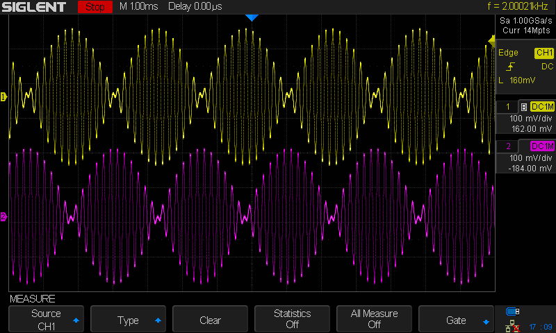
Figure 5: Primary coil 5 kHz, secondary coils at 200 Hz.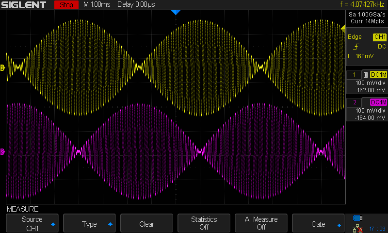
Figure 6: Primary coil 10 kHz, secondary coils at 100 Hz.
Figure 7: Primary coil 10 kHz, secondary coils at 200 Hz.TIPS
Do not overdrive the modulation input of the secondary coil generator with too much voltage. Around 10Vpp is enough to get full modulation without overdriving. Figure 8 below shows when too much voltage is applied to the modulation input (12Vpp). Figure 9 shows correct modulation depth (10Vpp).
Figure 8: Primary modulation voltage is too high. Note square edges of the waveforms.
Figure 9: Primary modulation voltage is correct. Note the smooth edges of the waveforms.Compare the modulation frequency of the primary coil and the modulation specifications of the secondary coil generator. If the modulation input of the secondary generator is low frequency, you may get “steps” in the output, as shown below:

Figure 10: Secondary coil signals with a primary coil frequency set too high.
Figure 11: Zoom of high frequency primary voltage. Note “steps” due to quantization.If this is the case, you can smooth the “steps” by placing low pass output filters on each of the secondary coil generator outputs.
This is very similar to filtering the images from a digital-to-analog (DAC) converter.The SDG1000X and SDG2000X have modulation sample clocks that are operating at 600 kHz. By adding a low pass filter with a pass band below the Nyquist limit for 600 kHz,
Design the filter such that the passband is below the 1st image frequency.

CONCLUSION
Simulating resolver outputs using arbitrary waveform generators provides an easy way to verify and troubleshoot the operation of resolver circuitry and software. The SIGLENT SDG1000X and 2000X series provide flexible and fast test instruments for this application.
REFERENCES
Infineon; (2016, December). DSD: Delta Sigma Demodulator [Web Article]. Retrieved from https://infineon.com
Szymczak, J.; et. Al (2014, March). Precision Resolver-to-Digital Converter Measures Angular Position and Velocity [Web Article]. Retrieved from https://analog.com
For more information, check Arbitrary Waveform Generators, or contact your local Siglent office.The basic output waveform and related parameters of the arbitrary waveform generator
Traditional function generators can output standard waveforms such as sine waves, square waves, and triangle waves. However, in actual test scenarios, in order to simulate the complex conditions of the product in actual use, it is often necessary to artificially create some “irregular” waveforms or add some specific distortion to a waveform. Traditional function generators can no longer meet the requirements and an arbitrary waveform generator may be a good option.
Arbitrary waveform generators can easily replace the function generators. They can source sine waves, square waves, and triangle waves like a standard function generator. In addition, they can also output pulse, noise, DC signal types, modulated signals, sweeps and bursts. Many arbitrary waveform generators currently on the market are equipped with arbitrary waveform drawing software. Through this software, theoretically, the arbitrary waveform generator can be remotely controlled to output all the signals required in the test process.
So, what types of waveforms can an arbitrary waveform generator output?
What parameters are available for an arbitrary waveform?
How to measure the quality of the output waveform?- Sine Wave / Cosine Wave
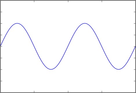 Figure 1 Sine wave / Cosine wave
Sinusoidal (sine) and cosine waves are the two most familiar waveforms in electronics.
Sine/cosine waves are defined as follows. (Formula 1)
OR
 (Formula 2)
Where A represents the amplitude of the sine wave,
 represents the angular frequency, and
  represents the initial phase, which can be omitted in the general calculation. The sine and the cosine waves are essentially the same, but the initial phase differs by 90 °.
 Figure 2 Sine wave setting interface in SDG1000X
Quickly Monitor FM Deviation using a Spectrum Analyser
Spectrum analysers are very useful tools for observing radio transmissions. One of the more common applications is to monitor a known channel or band of frequencies. In this note, we are going to show how to quickly capture an FM radio transmission and then configure the analyser to provide us with the frequency deviation of that signal.
NOTE: If you are unsure of the power of the signal that you are attempting to measure, it may be a good idea to add external attenuation to the RF input of the analyser to help prevent damage to the analysers sensitive measurement circuit. You are ultimately responsible for any damage caused by excessive signal power.
- Connect the appropriate antenna to receive the signals of interest:
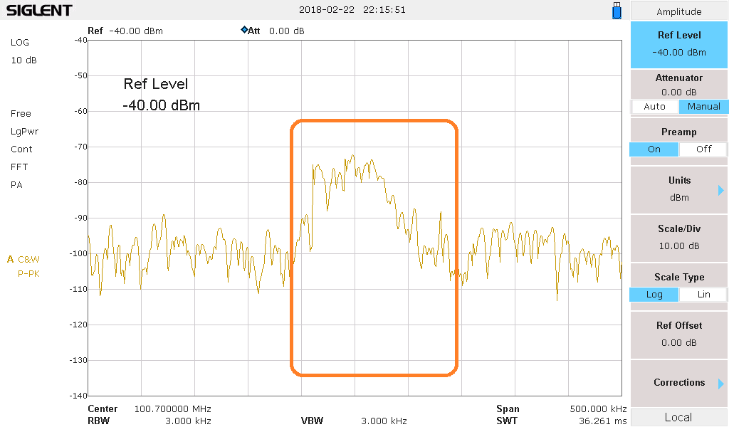
2. Press Frequency > Center Frequency and set the center frequency to match the frequency of interest. Here, we are setting the center frequency to 100.7 MHz, a local FM radio station:
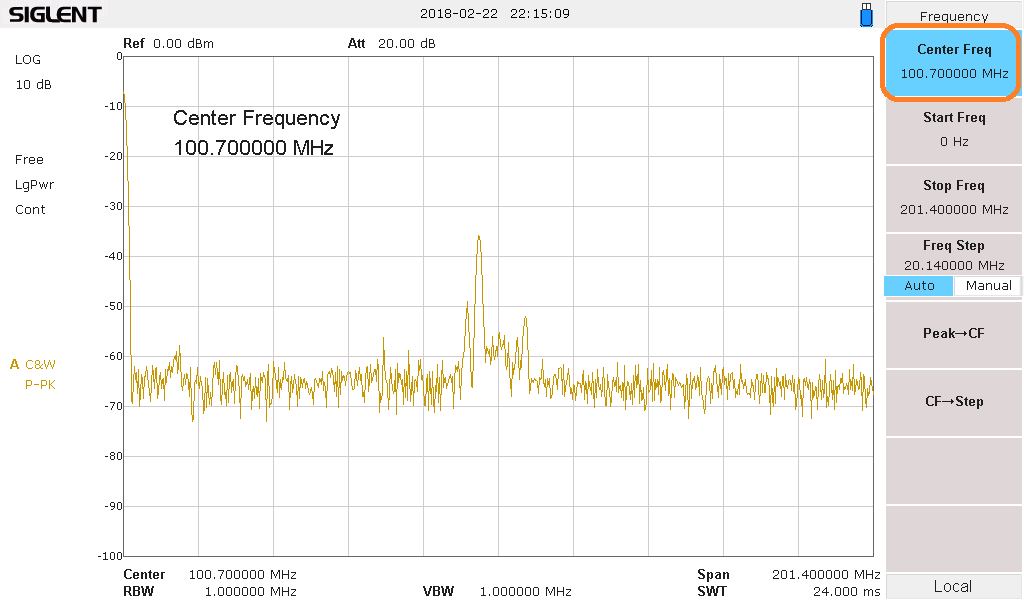
2. Press Span > Span and set the span to an appropriate level for your application. If you are looking at a single channel, you can set the span to 500 kHz or so. This will allow you to observe the channel and the full range of the frequency deviation:

3. If the signal is still very low or cannot be easily observed through the noise, you can lower the attenuation by pressing Amplitude > and lower the Attenuator setting. You can also enable the preamplifier.
NOTE: Use caution as lowering the attenuation and enabling the preamplifier makes the instrument more susceptible to damage due to overpowering the input.
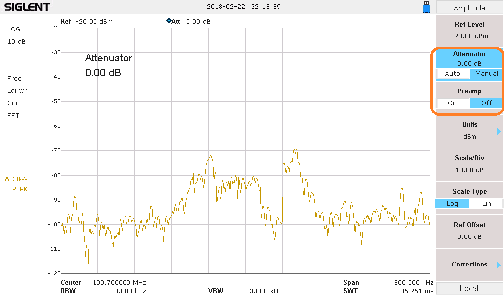
After adjusting the preamp and attenuator, you can see the signal rise out of the noise:
4. Now, we can activate another trace on the display and we can set it to be a Max Hold trace type. This trace type records the largest amplitude for each frequency bin and it will stay there until it has been manually cleared. Over time and successive scans, the Max Hold trace will show us the frequency deviation of our signal.
Note that trace 1 type is Clear Write. This overwrites each frequency bin amplitude with a new value for each scan:
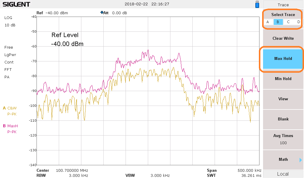
The FM deviation of this signal is approximately 4 divisions.
The Span is 500 kHz and there are 10 divisions on the display. Therefore, each division is 50 kHz. So, the FM signal deviates around 200 kHz.
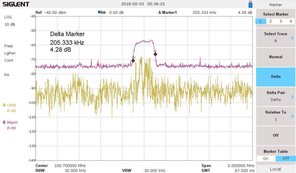
You can use markers for more accurate measurements:
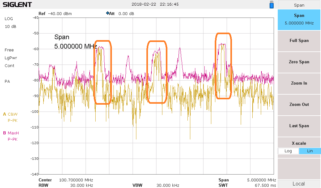
Or adjust the span to see adjacent transmissions:
Electromagnetic Compliance: Troubleshooting with Near-Field and Current Probes
Electromagnetic interference (EMI) can cause a host of problems, especially when developing a product or attempting to pass mandatory electromagnetic compliance (EMC) tests. Garbled displays, bad data, or complete malfunctions can occur when a design is effected by EMI. To minimise the effects of interference, government agencies like the Federal Communications Commission (FCC) in North America create and enforce standards that set limits on the EM output of a product type. Testing to the specifications is commonly referred to as Electromagnetic Compliance (EMC) testing.
Many EMC test failures stem from the interaction of unintentional radio frequency (RF) emissions with a circuit or element within the design itself. The electric and magnetic fields that cause this interference are not visible to the unaided eye, which can present complications when trying to isolate the root cause and minimize the effects of the EMI.
- What is causing the issue?
- Where is the source of the signal or energy causing the radiation?
- How can I fix it?
Fortunately, there are simple tools and techniques that can help identify the sources of EMI. Once you can identify the source, you can begin to build up a list of solutions to the problems. These techniques are not part of the mandatory compliance tests required to pass EMC testing. Rather, these are pre-compliance test techniques that help identify potential areas of EMI as quickly as possible without the burden of expensive test equipment and setups.
In this application note, we are going to introduce some common pre-compliance test techniques for identifying potential problematic EMI sources using near-field and current probes. These techniques can save you time and money by isolating problem areas quickly, and with a little fixturing, you can create repeatable test stations to help correlate data. This knowledge can then be used to “design for EMC” in your future products.
NOTE: Pre-compliance tests are designed to help identify and resolve issues that may hinder passing full compliance tests. Pre-compliance testing is not a replacement for full compliance testing at a certified lab.
ELECTROMAGNETIC RADIATION BASICS
In electronics, EM radiation is most commonly caused by a current flow or voltage build-up along or through a conductor. This includes traces on a PC board, discrete wires, component leads/pins, connectors, or any other metal, including the chassis, rack, or product enclosure. Recall that EM radiation is actually a combination of electric and magnetic field components. It is described as the propagation of orthogonal time-varying electric and magnetic fields as shown in figure 1.

Figure 1: Electromagnetic wave propagation out of the page (top left), to the right (top right) and out of the page at an angle. Note that the E and H fields are orthogonal (90°) to one another.
While the electric (E) and magnetic (H) fields are created by the same phenomena, they physically behave quite differently in the environment. Magnetic fields are only created by moving charges (current). In most circuits, current is conducted by traces on the PC board, component pins/leas, and discrete wires. Therefore, the magnetic field tends to dominate the EM radiation produced by the traces and wires that route signals and power to different parts of the design.
Visualising the magnetic field can be a bit easier if you go back to your Physics texts. Recall that the magnetic field of an infinitely long straight wire can be calculated by applying Ampere’s law:

For a circular path centered on the wire, the summation becomes:

Where:
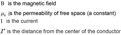
Figure 2 is a physical representation of this relationship. Note, this is also described by the “right-hand-rule” wherein if you were to point the thumb of your right hand in the direction of the current flow, then the magnetic field lines form concentric rings that wrap around the conductor in the direction of your fingers.
Figure 2: Magnetic field produced by a currentUnlike the magnetic field, electric fields can be created by moving or static charges. In this way, electric field effects dominate over magnetic fields when searching for EM radiation on surfaces like heatsinks or metal enclosures. The effects of the electric field also tend to dominate further away from the source (far-field). Far-field measurements are more susceptible to error due to environmental factors like radio stations, WiFi, and intentional RF. Far-field measurements, like those performed during radiated emissions portion of a compliance test, require more setup, equipment, and expertise than near-field.
By measuring the amplitude and frequency of the magnetic and electric fields that are generated by elements of a product, we can identify the areas that have the highest potential to cause EMI issues.
EQUIPMENT LIST
Here are the basic requirements for a near-field troubleshooting kit:
Spectrum Analyzer/EMI Receiver: Measures RF power with respect to frequency. The analyser should have a maximum frequency of at least 1 GHz, DANL of -100 dBm (-40 dBuV) or less, and a minimum RBW of at least 10 kHz.
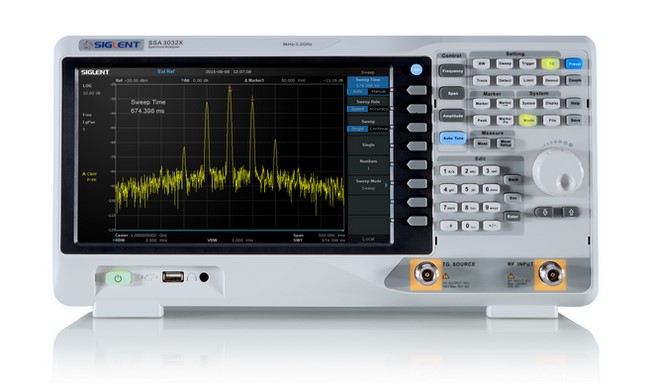
Figure 3: A SIGLENT SSA3021X 2.1 GHz spectrum analyser.Near-field probes: Commercial or handmade. Many are magnetic (H) field probes, but there are also electric (E) field probes as well.
Current probes: Commercial or handmade.
50 Ohm cable: Use a cable with connectors that mate to the near-field probes and the RF input of the spectrum analyzer. Many commercial probes can be purchased with a cable and any adapters that may be required.
PROBES
Since EMI cannot directly observed by the human eye, we need some tools to help. Recall that moving charges in a conductor produce magnetic and electric fields that radiate throughout space from the conductor. We can use these fields to induce a voltage in a circuit. Then, measure that induced voltage and therefore indirectly measuring the strength of the original field. The two most common types of probes used in EMI troubleshooting are near-field probes and current clamps.
Magnetic field probes and current clamps operate on a similar principle. The magnetic field that flows through the “loop” area of the probe induces a voltage that can be measured (figure 4). Larger loop areas pick up more magnetic flux, and are therefore better suited to finding smaller signals, but smaller loops offer better spatial resolution. Many kits come with multiple loop sizes (figure 5) to help strike the balance between sensitivity and spatial resolution.
Electric field probes do not generally have a loop area. They pick up the electric field similar to a monopole antenna. The rotation of an electric field probe is not critical as with the magnetic field probe, but the distance from the signal source is.
Here are some guidelines for probing:- Measure the background radiation by powering off the device-under-test and monitor the analyser display. Note any RF that may be caused by background or environmental conditions and retest often.
- Probe displays, communications port terminals, and any cutout/air vent/seam of the enclosure. These are common problem areas.
- E and H field probes positioned closer to the signal source will measure higher amplitudes
- H field probes oriented perpendicular to the magnetic field will measure higher amplitudes than those oriented parallel to the magnetic field.
- Since probe positioning is critical to repeatable measurements, a non-conductive fixture (wood, plastic) to position the device-under-test (DUT) and the probe can be used. Remember, position and orientation are very important. A few millimeters or a few degrees of rotation can cause a big difference in the measured amplitude of a given magnetic field.
 Figure 4: Magnetic field probe orientation and position affect measurement amplitude.
 Figure 5: SIGLENT SRF5030 near-field probe kit.
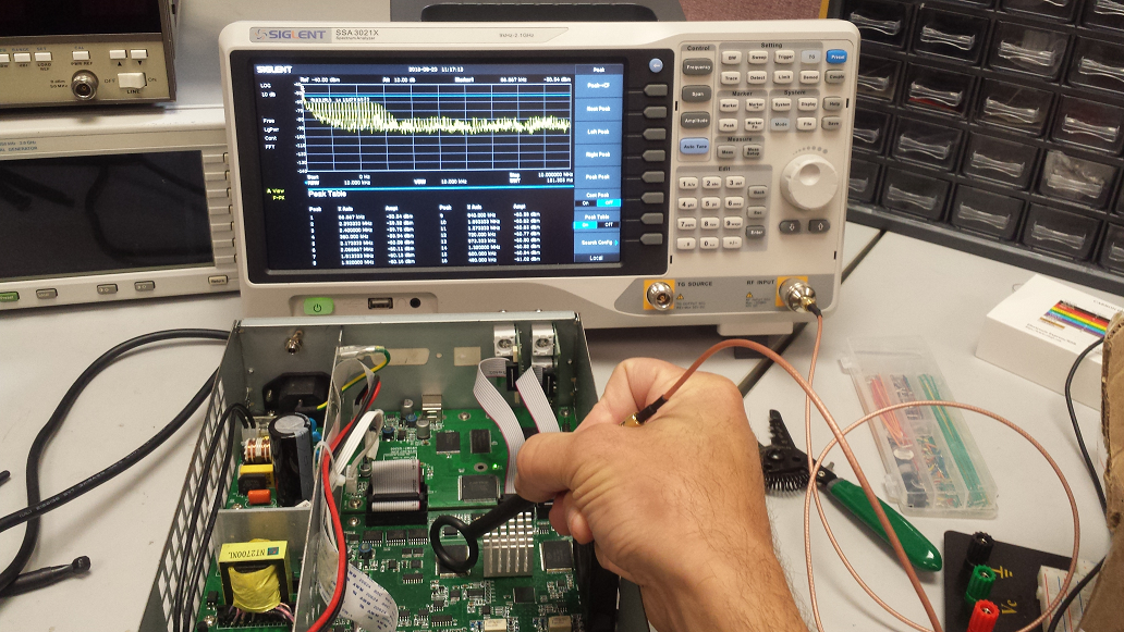 Figure 6: Probing a PCB using a SIGLENT SSA3X and SRF5030 probe.
Cables and interconnects can make very effective (and unintentional) antennas if they are not shielded/grounded correctly. Small currents flowing on the outside of the conductor can easily cause radiated emissions that can exceed the set EMC limits. A current clamp can be used with a spectrum analyser to provide insight into the cause of radiating cables/interconnects.
Current clamps operate on the same principle as magnetic loop probes. They can be purchased or made by wrapping a few rounds of wire around a ferrite clamp and epoxy a BNC connector as shown in figure 7. Simply attach the clamp to the cable to be tested, connect it to the spectrum analyser input, and configure the analyser for the frequency span of interest.
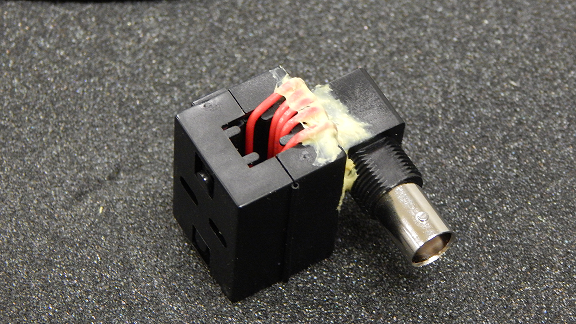
Figure 7: A handmade current clamp.Here are some guidelines for probing:
- If in doubt, add an external attenuator to the RF input of the analyser before you start. Power cables or expected high-power applications can have signals that will damage the sensitive RF input of the analyser.
- Test all of the cables that could be connected to the DUT. This includes the power cord, USB, Ethernet, and any other possible connections (figure 8)
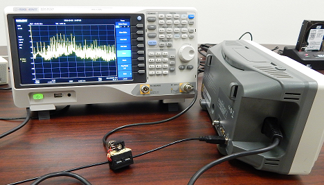
Figure 8: Measuring the RFI of a USB cable connected to a scope.- Current clamps, especially handmade, are susceptible to picking up environmental RF that can skew or overwhelm the signals that you wish to measure. Connect and arrange all cables, probes, etc.. and then measure the environmental RF by simply keeping the DUT powered OFF. Then, compare it to measurements made with the DUT ON. It may also be a good idea to retest periodically to account for any environmental changes.
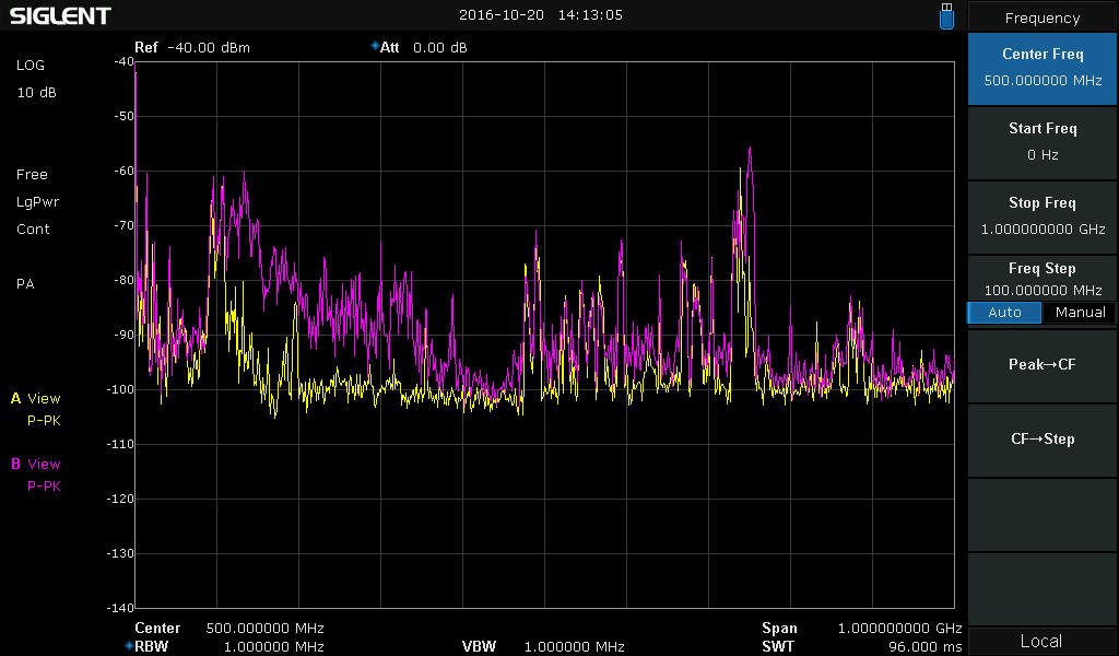
Figure 9: Traces of the environmental pickup from a current clamp (Yellow) and with the DUT powered ON (Pink).- If you have a failed radiated emissions report, start by looking for the failed frequencies or for the first few harmonics of those frequencies.
SCANS AND EVALUATION
It is highly unlikely that data collected during probing will directly correlate to radiated emissions test performance. But, by observing the RF output of cables, switching power supplies, displays, and cutouts, you can have information that can lead to faster troubleshooting if you do happed to fail.
Here are optional techniques that can help provide more insight:
1. Most spectrum analysers do not have pre-selection filters. If you are using a spectrum analyser without pre-selection filters, the peaks you observe may not be real. Analysers without pre-selection filters can create false peaks due to out-of-band signals mixing with the observed signals.
You can test the validity of a peak by adding an external attenuator (3 or 10dB should do). Real peaks will fall by the amount of the attenuator. If the peak falls by more than the attenuator, it is likely to be a false peak. Make a note of the false peaks for comparison with your compliance test results. You can also use pre-selection filters or an EMI receiver, but these tend to be cost prohibitive for most quick testing.
Figure 10 below shows a typical peak confirmation test. The yellow trace was collected without an attenuator. The Pink trace was collected with a 10 dB attenuator added to the RF input of the analyser. In this case, the peaks drop the same amount as the added attenuation. This helps affirm that the peaks are likely real and not products of out-of-band signals.

Figure 10: Comparison of two scans using the marker table function of the SIGLENT SSA3000X spectrum analyser. The Yellow trace was collected without attenuation while the Pink trace was collected after adding a 10 dB external attenuator.2. Many spectrum analysers have Max Hold trace types that will continuously hold the highest amplitudes of each frequency scan. You can enable a single trace as Clear Write to show active RF performance and enable a second trace as Max Hold. This allows you to compare changes in the DUT to the “worst case” data collected and “frozen” using Max Hold.
3. You can use markers and peak tables to clearly indicate peak frequencies and amplitudes, if available.
Figure 11: SSA3000X analyzer with Peak table and markers activated.CONCLUSION
- Magnetic fields are produced by current flow. Use a magnetic (H) near-field probe to identify EM radiation near traces, wires, and ribbon/flex cables.
- Electric fields can be produced by current flow or static charge build up. Use an electric (E) near-field probe to identify EM radiation on metal surfaces like heat-sinks, enclosures, display bonding/edges, and slots/cutouts.
- Use current clamps to identify potential radiation and resonance from cables, wires, and interconnects
- Displays, cutouts/holes/seams in the chassis, ribbon cables, and communications ports/busses are the most likely cause of radiated emission failures.
- Use conductive tape or aluminium foil to cover areas of “leakage”, making sure that the covering is grounded. Rescan with the tape/foil in place to see if it has mitigated the EMI.
- Poorly terminated cables and interconnects also cause radiated issues
- Frequently measure the background effects by removing power from the device-under-test and monitor the output on an analyser. Note any changes and their potential effects on the measurements.
With a few simple tools, you can implement an in-house pre-compliance test process that will minimize the total development time for your products, lower the cost of design, and decrease the amount of testing on future products.
Spectrum Analyser Basics: Bandwidth
Spectrum analysers are useful tools for broadcast monitoring, RF component testing, and EMI troubleshooting. There are a number of common adjustments available with many modern analysers that can optimize performance for a particular application. In this application note, we will introduce resolution bandwidth (RBW) and video bandwidth (VBW) and how they affect measurements.
Resolution Bandwidth (RBW)
Bandwidth is defined as the span of frequencies that are the focus of a particular event. For example, the bandwidth of transmission signal is the span of frequencies that the transmission occupies. The bandwidth of a measurement defines the range of frequencies that were used for the measurement.
In spectrum analysis, the resolution bandwidth (RBW) is defined as the frequency span of the final filter that is applied to the input signal. Smaller RBWs provide finer frequency resolution and the ability to differentiate signals that have frequencies that are closer together.
Why not use the smallest RBW setting for all measurements?
Sweep Time.
Sweep time is the length of time it takes to sweep the detector from the start to the stop frequency. Here is the equation governing the sweep speed:

In this formula, the meaning of the first factor is the number of frequency selections under SPAN, each step is 1 / k of RBW, to ensure the accuracy of amplitude measurement. The second factor means that each selection The time required depends on the smaller value between RBW and video bandwidth (VBW). Usually when we do not focus on noise, the VBW can be set to a value greater than or equal to RBW.
The time equation is reduced to:

That is to say, the scanning time is proportional to SPAN and is inversely proportional to the square of RBW. This means that if the RBW is reduced by 100 times the scanning time will be increased by 10000 times in the same SPAN
Smaller RBWs also lower the noise floor, but they extended the sweep time for a given span of frequencies. Select a spectrum analyser that has a large number of RBW settings, especially on the lower frequency end. You may not use 10 Hz RBW often, but it is very useful when you do. Adjustment is easy. Simply adjust the RBW to provide the proper balance between speed and resolution for your application.
Figure 1 is the measurement of two signals separated by 20 kHz. The traces were collected using RBWs of 30 kHz (Blue), 10 kHz (Yellow), and 3 kHz (Pink). Observer that while the frequency of these two similar signal measurement power is completely unchanged, the signal separation is only clear when the RBW is less than the frequency difference between the signals.
Figure 1: Spectrum analyser display showing two signals at three different resolution bandwidth (RBW) settings.Shape and Shape Factor
The shape and shape factor of the RBW filter can also be an important selection. Many analysers have an RBW filter that has a Gaussian shape and a shape factor determined at the 3 dB point. The RBW value is the bandpass frequency of the filter 3 dB below the peak response of the filter. Recall that 3 dB is equal to 50% of the maximum. This is also referred to as the filters Full Width Half Max (FWHM) value. The 3 dB Gaussian filter is acceptable for many measurements, but for Electromagnetic Compliance (EMC) related measurements, a filter defined at 6 dB may be required.
The shape factor of a filter is the ratio of the response at two attenuation values. Typically, the highest attenuation is measured at 60 dB down. The lower attenuation value is either or 6 dB down. It is a measure of the sharpness of the filter response. If the ratio is large, the filter is not very “sharp”. This indicates that the filter spreads out over a large frequency range. If the ratio is small, this indicates a skinnier filter shape and sharper roll off. This aids in rejecting more out-of-band signals because they don’t “bleed” over. Figure 2 shows how the shape factors for both the 3 dB and 6 dB points are calculated for a given filter. For spectrum analysers, the 3 and 6 dB shape factors are similar, but the 6 dB filter has a steeper curve and has higher out-of-band rejection.
Shape Factor @ 3/60dB = (F6 – F1)/(F4-F3)
Shape Factor @ 6/60dB = (F6 – F1)/(F5-F2)
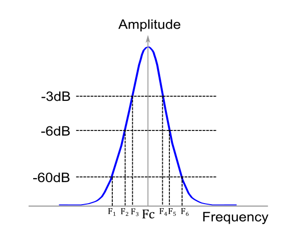
Figure 2: Gaussian filter showing 3, 6, and 60 dB points and center Frequency (Fc).Phase Noise
Another factor that affects the frequency resolution of an analyser is the phase noise. This is observed as a widening and increase in the noise amplitude near the center frequency of the signal (figure 3). It is caused by the random thermal fluctuations of the oscillator used as a timing reference in the spectrum analyser circuitry. These fluctuations cause the phase of the output clock signal to vary with time, very similar to jitter in a time-based system. This widening can cover up any small signals that may be near the frequency of interest. For meaningful measurements, select an instrument with lower phase noise than the signal source you are measuring.
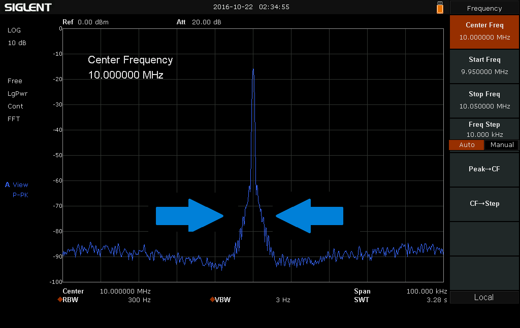
Figure 3: Spectrum analyser display showing phase noise effects of an input signalVideo Bandwidth (VBW)
Another factor that affects the displayed trace quality of a spectrum analyser is the video bandwidth (VBW). Video filtering is a time-domain low-pass filter, mathematically equivalent to the mean or average. The main effect of the VBW filter is to smooth the trace and decrease noise.
Strictly speaking, the VBW does not change the measurement results. It will not affect the “frequency selection, peak detection” of the measurement process. The VBW filter is applied after the data has been collected, but before the screen displays the trace. As can be seen from figure 4 below, when the VBW is large, noise makes small signal observation difficult. If we reduce the VBW, the small signal becomes much more clearly.
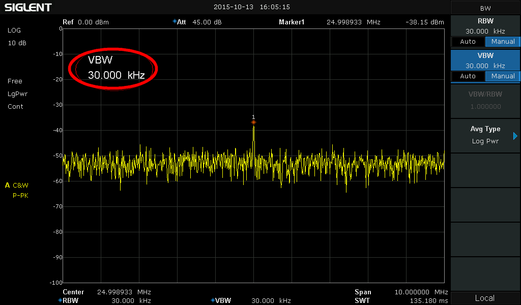
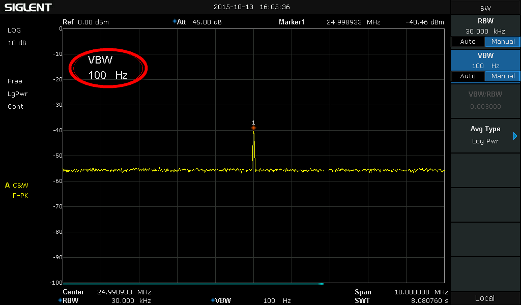
Figure 2: Smoothing effect of random signal with different VBWConclusions
Modern spectrum analysers offer flexible measurement capabilities. Select an analyser that provides an adjustable RBW/VBW (lower is better), lower phase noise than the signal you are testing. Adjusting the RBW can provide lower noise floor and fine frequency resolution, but the sweep time will increase dramatically. For noisy signals, you can lower the VBW to help smooth the trace and make signal identification easier, but this will also increase sweep time. If you are performing EMI measurements, a 6dB sharper filter option is required to increase peak detection accuracy.
Spectrum Analyser Basics: Detectors
Spectrum analysers like the SIGLENT SSA3000X Series have a number of available detector selections that can help you observe specific signals of interest. This operating tip provides a brief description of the available detector types and suggested usage.
BASICS:
The SIGLENT SSA 3000X Series spectrum analysers normally display power versus frequency on a Cartesian coordinate system as shown below:
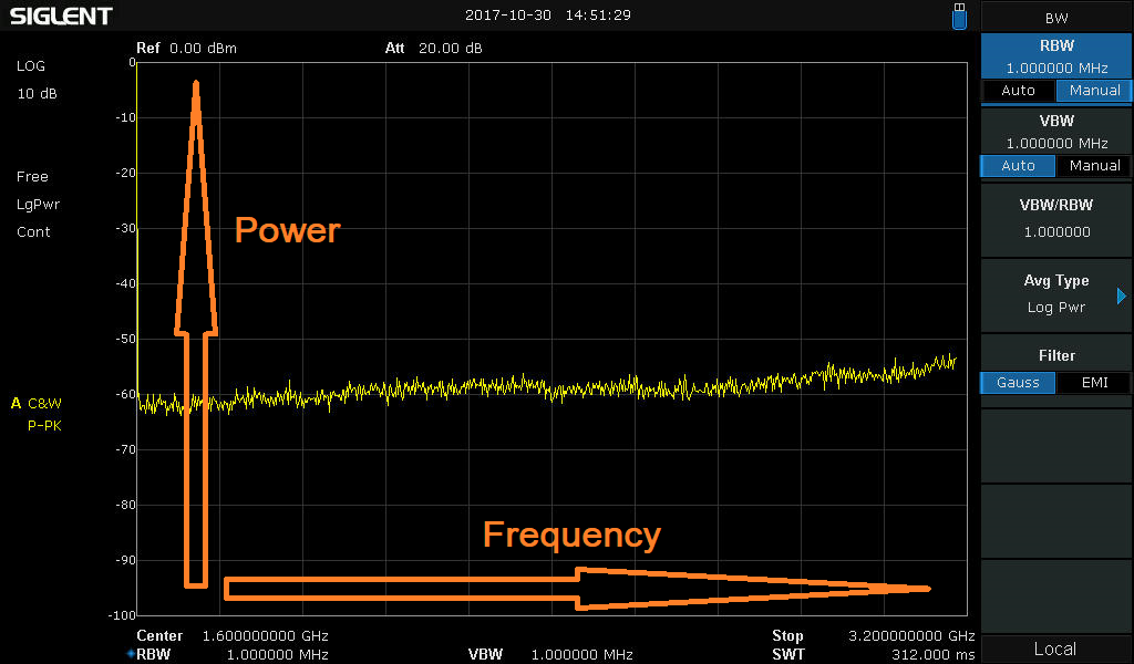
The horizontal span (which composes a frequency span when the instrument is configured to sweep/not in zero span mode) is comprised of 751 discrete samples (also called “bins”).
The analyser sweeps from the start frequency to the stop frequency and fills each frequency “bin” with an amplitude value determined by the detector selected for that particular sweep operation.
THE DETECTORS:
Positive Peak: For each trace point, a Positive Peak detector displays the maximum value of data sampled within the corresponding time interval.
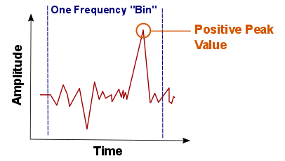
Positive peak detectors are the most commonly used detector type. They are perfect for measuring the peak power of a signal as well as determining the “worst case” signal in EMI applications.
- Negative Peak: For each trace point, a Negative Peak detector displays the minimum value of data sampled within the corresponding time interval.
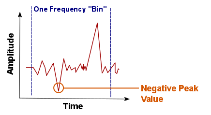
Negative peak detectors are rarely used, but can be helpful when comparing positive and negative peak values when looking for CW and Pulsed signals. CW signals will have less difference between positive and negative peak values for a given frequency bin. A pulsed signal could have a significant difference
- Sample: For each trace point, a Sample detector displays the transient level corresponding to the central time point of the corresponding time interval.
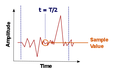
This detector type is applicable to noise, noise-like signals, or small amplitude continuous wave (CW) signals that are near the noise floor of the analyser.
- Normal: Normal detector (also called rosenfell detector) displays the maximum value and the minimum value of the sample data segment in turn; namely for an odd-numbered data point (bin), the maximum value (positive peak) is displayed; for an even-numbered data point (bin), the minimum value is displayed. In this way, the amplitude variation range of the signal is clearly shown.
- Average: For each trace point, an Average detector displays the average value of data sampled within the corresponding time interval.
- Quasi-Peak (QP): This is a mathematically weighted form of the positive peak detector. For a single frequency point, the detector measures the peaks within the defined detector dwell time. These peaks are then weighted using a mathematical model that simulates a tank circuit that meets charge/discharge rates specified by CISPR (an international organization that governs electromagnetic effects). The measurement time for QPD is far longer than Peak Detector.
For a given signal, the QP detector values will never be greater than the positive peak results.
Electromagnetic Compliance: Measuring Conducted Noise with a Tekbox LISN
Our friends at Tekbox have a nice app note that provides details on performing conducted noise measurements using a SIGLENT SSA3000X Spectrum Analyser: