Your cart is currently empty!
Author: James
DC Power Supply Sinks Current when Output is Turned Off
When using a DC power supply for charging a load such as battery or capacitor, it is important to note that the DC power supply absorbs a current from such loads when the output is turned off. Here we are going to further explain this power supply’s behaviour; DC power supply, in general, comprises a bleeder circuit to discharge a power supply’s electrolytic capacitor at its output terminal. If the output is turned off after charging a battery or capacitor, the bleeder circuit sinks the current from them. The purpose of the bleeder circuit is to quickly discharge the voltage stored in the power supply’s electrolytic capacitor for safety reasons.
Now look at the following figures. Figure 1 shows the equivalent circuit of the DC power supply output and Figure 2 shows the example of the sink current measurement. This example data may help you estimate a discharge current and voltage change of your load.
1. Equivalent Circuit of DC Power Supply: When output is turned off
As shown in Figure 1, the sink current (shown in red arrows) flows through the 39-kΩ resistance and voltage-following constant current circuit (CC varies by voltage).
Sink current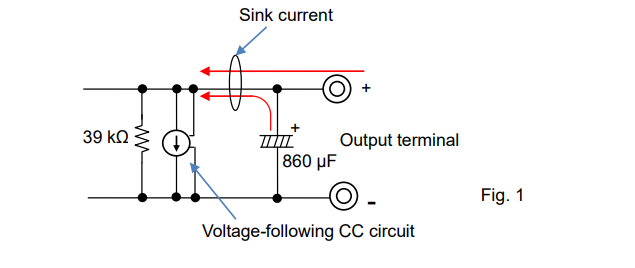
2. Sink Current: When output is turned off
Figure 2 is the example of the sink current measurement through above resistance and circuit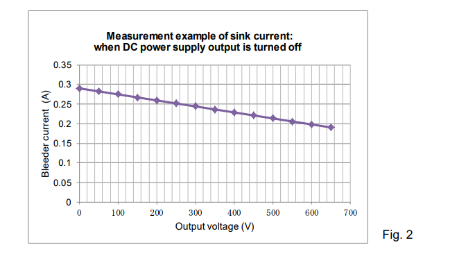
When the DC power supply is turned off, the sink current flows through the 39-kΩ resistance only.
Products Mentioned In This Article:
- DC Power Supplies please see HERE
How to use the voltage correction function on frequency response
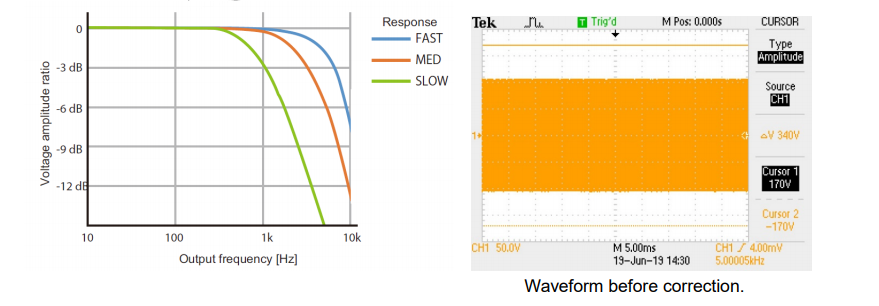
The PCR-WE can output up to 5 kHz, but it has frequency response as shown in the figure below. The response is about -3dB at 5kHz. For example, the waveform in the figure below is for 120 Vrms, 5 kHz.
Voltage amplitude correction
The PCR-WE has a function to correct the attenuation due to the frequency response of the output. Please refer to the “The soft sensing function is used” page of the User’s Manual.
Steps to enable features:
1. Turn off the Output.
2. Set the Output Voltage.
3. Press Oher button (Shift + Memory) > 1/2 (F6) > COMPEN (F2) > SENS.-S (F3).
4. Press ENT.
“SENS.-S” is displayed on the panel.
5. Press 1/2 (F6) > SOFT.SENS (F2) > S.POINT (F5) > O.TERM (F2)Set the sensing point in output terminal. 6. Press ESC > V.CTRL (F2) > AC (F2)
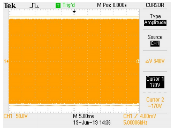
Corrected waveform
The output voltage is 120 Vrms.Products Mentioned In This Article:
- PCR-WE Series please see HERE
DC Electronic Load – Part 1: What is a DC Electronic Load?
Beginners who have never used an electronic load may well get confused with the difference between electronic loads and power supplies. They sometimes wonder ‘why the electronic load does not provide any output…?’
While similar in appearance, electronic loads are totally different from power supplies. It is not often you get to see them but it is suitable for specific applications such as working as variable resistors, in a part of high-power systems, to test power supplies.
From here we offer a great series of white papers that give you a thorough understanding of the basics and use of electronic loads, ranged from what it is through to how it is used including its operating principle. Part 1 explores the fundamentals of electronic loads.
* This series focuses on explaining DC electronic loads only; AC electronic loads will not be included.
1. Fundamentals of DC Electronic Load
DC electronic loads are used in a range of DC power supply tests. We will discuss why they are ideally suited for power source testing, in contrast with a popular device, DC power supply.
1-1. Electronic Load and Load of Horse-Drawn Vehicle
Electronic loads can help you investigate the ability of power supplies. This can be compared to the method of determining an ability of a cart horse. Figure 1-1 shows that the horse is pulling the cart of mass 490 kg (approx.1080 lb). If the horse cannot pull a cart of mass 500 kg (approx. 1102 lb), it proves that this horse has the ability of pulling the cart up to 490 kg (approx.1080 lb).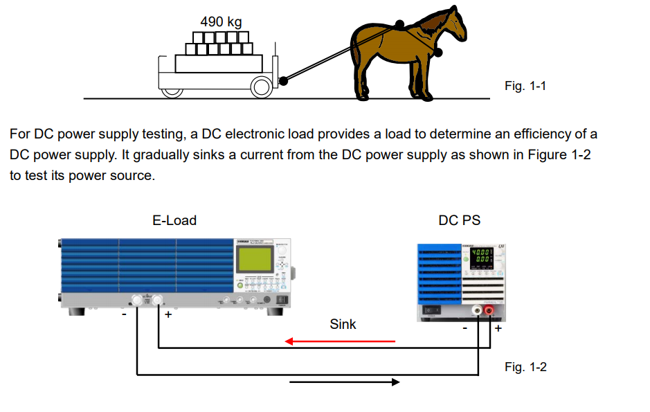
You now understand how electronic loads are different from power supplies; power supplies apply a voltage to DUTs, while electronic loads sink a current from DUTs. So you can now really understand the answer to ‘why electronic loads do not provide any output…?’
1-2. Act as Substitute for High-Power Components
Electronic loads are used to test power source devices. According to Ohm’s law, if the resistor is connected to the output of the power source device (DUT), the current flows from the DUT (See Figure 1-3). Electronic loads can be used as substitute for the resistor. Furthermore, users can easily adjust the resistance value on their own from electronic loads.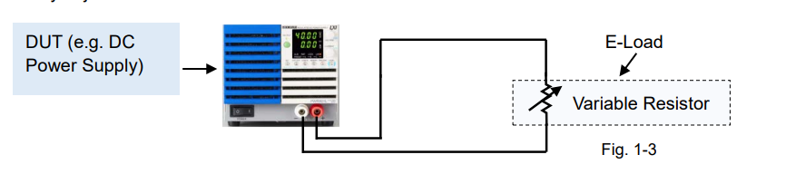
In other words, electronic loads can act as a variable resistor, and also achieve tens of kilowatts of power. Instead of using different sizes of fixed resistors, one unit of electronic load allows you test the load dynamically in a repeatable fashion.
Electronic load circuits regulate the resistance value. Based on the performance of circuit functions, electronic loads behave like a 1) Variable resistor 2) Variable Zener diode 3) Load simulator, which described in more detail in the following sections.
1) Act as Variable Resistor
Figure 1-4 shows that the variable resistor is connected to the DUT.
Figure 1-5 shows the relationship between the voltage (V) across the resistor and resistor’s current (I). This relationship in a circuit of the resistor produces a straight line. In the graph, the resistance (R) is the slope. The slope varies according to the resistance value.
During the DC power supply tests, the electronic load controls the resistor’s current by adjusting the resistance value.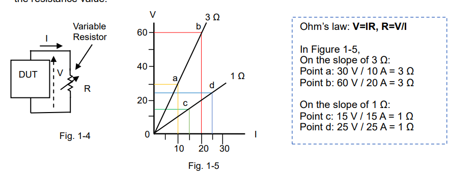
The most important aspect is that “the variable resistor can regulate the current flow in the circuit.” If the electronic load acts as a variable resistor, it means that you can control the current based on your test applications or conditions with electronic loads. Furthermore, electronic loads have a capability to provide a constant power or constant current mode, which are described in the next article.
2) Act as Variable Zener Diode
Figure 1-6 shows that the Zener diode is connected to the DUT.
Figure 1-7 shows the relationship between the voltage across the Zener diode and its current. Once the voltage reaches a certain point known as the Zener voltage (Vz), the Zener resistance dramatically decreases. The Zener diode clips any voltage that exceeds the Zener voltage (Vz). In an electronic load, you can set a voltage (equivalent to the Zener voltage) that remains constant regardless of changes to its input current (I). This set voltage is called the constant voltage (CV) and this operation is called the CV mode.
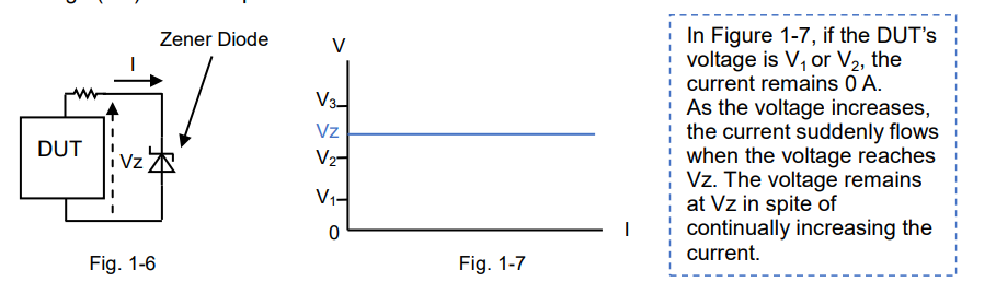
If the DUT is motor in figure 1-6, the DUT may provide a regenerative power by reversing the direction of the motor rotation and it may cause a reverse voltage spike. To prevent it, set the CV voltage so that the voltage will not exceed this CV set voltage.
3) Act as Load Simulator
High-performance electronic loads can simulate various power states so they can be used in diverse applications instead of using a real load. You just select an appropriate electronic load that can exactly simulate your actual load with the waveforms in the example below;
Figure 1-8 shows that the test waveform current flows on a circuit.
Figure 1-9 shows the current waveform simulation example for lamp current.
Figure 1-10 shows the pulsed current waveform simulation example.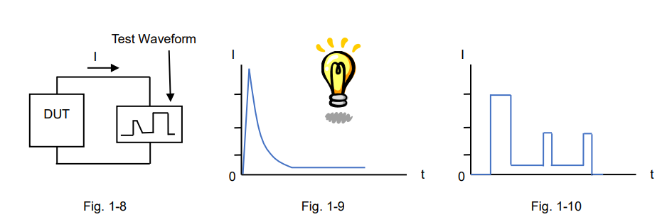
Products Mentioned In This Article:
Kikusui Electronic Loads please see HERE
Two Methods to Absorb Motor’s Regenerative Current Using Electronic Load
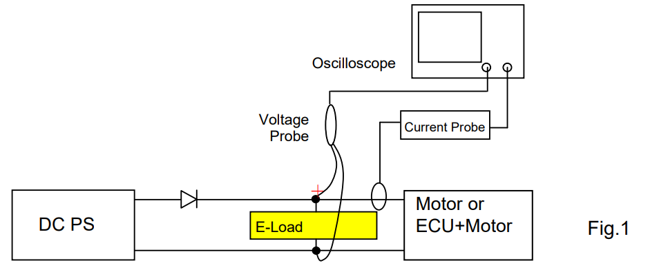
There are two methods to absorb motor’s regenerative current; Voltage Clipping Method and Bleeder Method. The following describes the characteristics, functions and precaution for the methods. Fig.1 illustrates the typical test system.
1. Voltage Clipping Method
This method is to set the electronic load in CV mode to clip the motor’s regenerative current. If the regenerative current is not fully followed, overshoot may occur even with this method. The overshoot occurs depending on the relationship between the rise time of regenerative current and CV switching time of electronic load:
-The faster the CV switching time is, the more voltage can be saved.
-Motor impedance determines the rise time of regenerative current. The larger the impedance is, the slower the rise time of regenerative current becomes.
This allows CV switching to perform properly, and the overshoot can be suppressed.1-1 Response Time for CV Mode with Typical Electronic Load
The following are the response time for CV mode with PLZ205W. In PLZ-5W Series, you can choose two modes for CV switching. Fig.2 is for Fast mode, Fig.3 is for Normal mode. Measurement Condition:
– 15V is set to PLZ205W for the CV setting.
– When approx. 12V is applied to PLZ205W, PBZ60-6.7 applies rapid constant current (approx.30μs).
The yellow line shows when the voltage was clipped: Fast Mode: approx. 300μs Normal Mode: approx. 3ms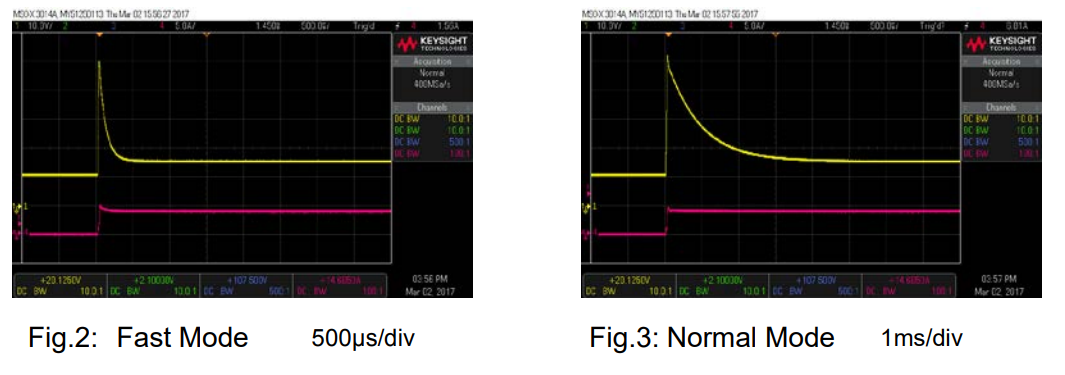
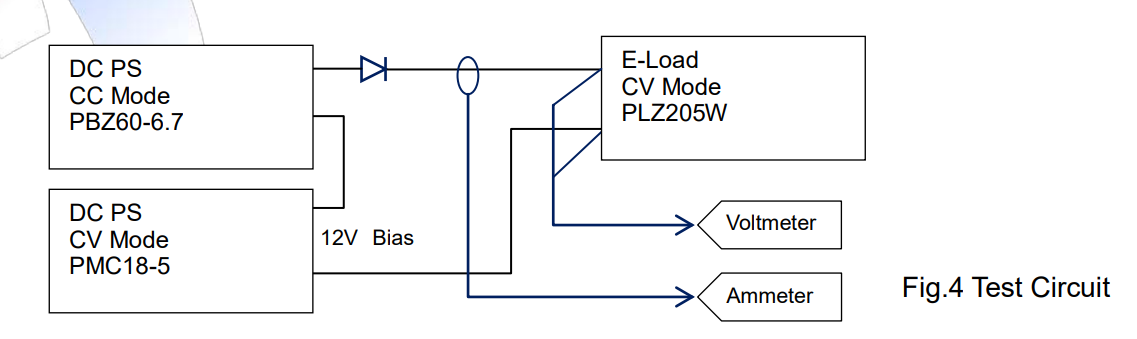
In Fig.2 and Fig.3, the overshoot voltage was much high. It is because PBZ60-6.7 applied 60V and the rise time of current is fast (approx. 30μs). Fig.4 illustrates the test circuit.
1-2 Precaution in use
Since impedance varies by motor, pre-test is recommended to check whether: – Overshoot is clipped until it meets your satisfaction.
– Oscillation occurs depending on the combination and compatibility between the motor inductance or load cable inductance and electric load.
2. Bleeder Method
This method is to set the electronic load in CC mode to always flow the higher current than regenerative current into the electronic load. When the regenerative current flows, the voltage of electronic load becomes higher than the power supply voltage. In such condition, the power supply current is cut off and the regenerative current flows into the electronic load to clip the regenerative voltage.
To drive the motor:
– Power supply should have the output current capacity for ‘motor drive’ + ‘regenerative current’. – At least the same amount of regenerative current should be always flowed into electronic load. Fig. 5 shows the result to clip the regenerative current with this method. This test circuit is shown in Fig.1.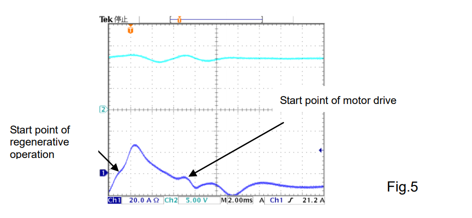
The merit of this method is that you can clip the voltage without overshoot. On the other hand, the current of electronic load for the regenerative current is continually being wasted. Therefore, please be noted that the system consumes quite a large power.
Products Mentioned In This Article:
- Kikusui Electronic Loads please see HERE
Choosing Electronic Load that Best Fits Your Switch Testing System
The switch on/off testing can be performed with a combination of DC power supply and electronic load (See Figure 1). To successfully conduct the testing, it is important to know that the current flow through the switch varies by the electronic load specifications or settings. Especially during the life testing, you should be aware that it may affect the lifetime of test switch.
This white paper shares the measurement results using our different electronic loads and helps you understand how to choose or set an electronic load for your switch testing system.1. Switch Testing System Configuration and Test Conditions
Figure 1 shows the system configuration diagram for the switch on/off testing.
Test Conditions: Set DC voltage to 14.6 V by DC power supply. Set PLZ150U or PLZ70UA in CC or CR mode.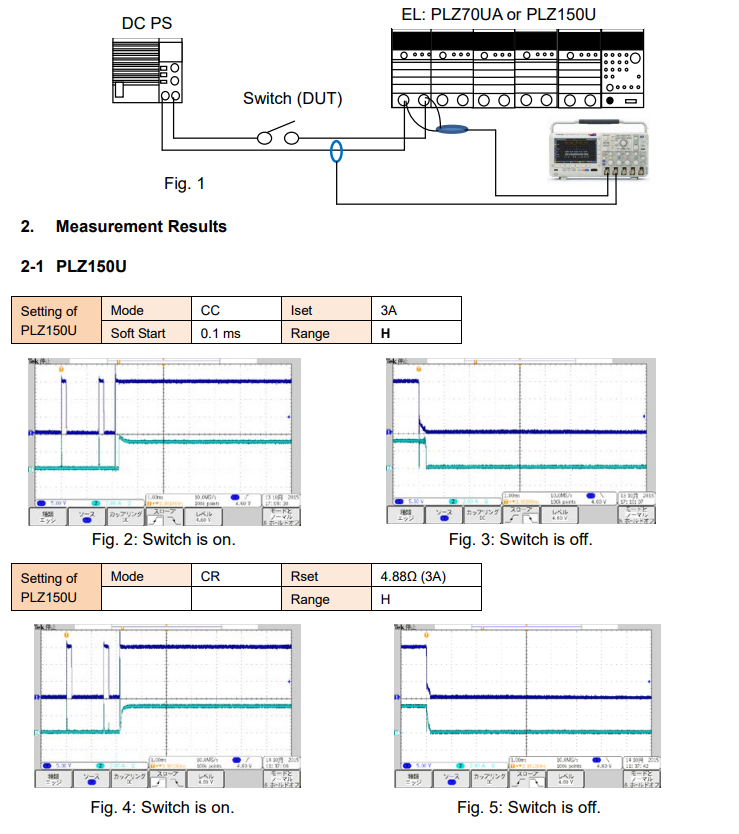
3. Important Points for Switch Testing System
Consider the following points when preparing the testing system;
1) Almost no current is supplied during the chattering at switch-on (See Fig. 2, 4, 6 and 8). *1
2) Set Soft Start to 0.1 ms to start the current flowing as soon as possible.
3) The magnitude of current differs in CC mode and CR mode at switch-off. Higher current can flow in CC mode (See Fig. 3, 5, 7 and 9).
4) Connecting an electrolytic capacitor in parallel with the electronic load input is also effective to simulate the start-up inrush current (switch-on surge). With the capacitor, very little voltage will be applied on the both side of the switch at switch-off.
5) Set the CV value (+CV mode) if using 0 V input operating voltage type of PLZ Series, such as PLZ70UA, PLZ164WA or PLZ664WA.
*If the power supply’s output is turned off first, the electronic load may cause an alarm. Turn off the electronic load first and then turn the power supply’s output off.
6) Overcurrent testing can be also performed in the same system; Use an electronic load whose capacity is large enough.
Under the above test conditions, PLZ150U can provide the better results than PLZ70UA.
*1: The Soft Start function is gradual starting up of an electronic load to avoid the overshoots of current. While the short-pulse voltage is first applied to an electronic load during the chattering, the Soft Start will minimize large startup currents from flowing. It delays the current start-up time for approx. 0.1 – 0.2 s.Products Mentioned In This Article:
- Kikusui Electronic Loads please see HERE
How to use the power line disturbance simulation function of PCR-WE
Voltage dips, short interruptions and voltage variations immunity tests of the IEC 61000-4-11 standard can be easily tested using the power line disturbance simulation function of PCR-WE.
As an example, it explains how to set the voltage dip test. You can easily execute tests under the test conditions specified in the standard in a few steps.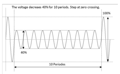
IEC61000-4-11 Voltage dip
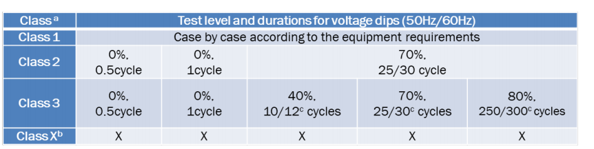
a Classes as per IEC61000-2-4; see Annex B.
b To be defined by product committee. For equipment connected directly or indirectly to the public network, the levels must be less severe than Class 2.
c “25/30 cycles” means “25 cycles for 50Hz test” and “30 cycles for 60Hz test”Simulation setup procedure
First, determine the exam level and duration.
Let’s create a simulation waveform of 0.5 cycle with 0% voltage amplitude of Class 2. (As an example, the test voltage and frequency are 120V 60Hz.)
The duration is 0.5 cycle, so it is 8.3ms (= 0.5/60Hz). The test level is 0%, so it is 0V.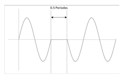
Next, set the simulation function.
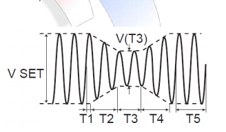
1. Set the steady-state voltage and frequency. (ex. 120V 60Hz)
2. Press SIM>COND(F4) to set the conditions.
3. POL ”+” / T1 TYPE “TIME” / T5 TYPE “TIME”
4. Press ESC to return to the previous screen.
5. Press EDIT(F5) to set the parameters.
6. T1 ”0” / T2 “0” / T3 “10ms“ / T4 “0” / T5 “10s” / T3 VOLT “0”
7. Press ESC to return to the previous screen.
8. Select LOOP(F3) to set the number of repetitions. (ex. 3 times) Configuration is complete.Press SIM > RUN (F1) to execute a power line disturbance simulation.
Using a trigger out signal makes it easier to observe the waveform with an oscilloscope.Products Mentioned In This Article:
- PCR-WE Series please see HERE
How Does Surge Suppression Work in PCR-LE/LE2 Series?
PCR-LE/LE2 Series feature the Surge Suppression function that involves the process of protecting PCR-LE/LE2 from voltage spike.
You can choose Surge Suppression to turn on or off depending on your load condition. If you want to avoid any voltage overshooting or undershooting, always set Surge Suppression to on. However, when you use a load with regenerative feedback (e.g. capacitive load or battery), it is recommended that Surge Suppression is set to off. In this white paper, we are going to provide the details of Surge Suppression function and make clear the difference between when Surge Suppression is set to on and off.
1. Surge Suppression: On
Surge Suppression is set to on as factory default.1-1. Timing Chart
Figure 1 shows the timing chart when Surge Suppression is on;
1. The output is in the high impedance state while the output is turned off.
2. When the output is turned on, the voltage stays at 0 V for first 200 microseconds, and then the voltage rises to the set value.
3. When turning off the output, the voltage firstly falls to 0 V for approx. 200 microseconds, and then the output stays in the high impedance state.
Thanks to this ‘staying at 0 V for approx. 200 microseconds’ behaviour, Surge Suppression can prevent the voltage overshooting or undershooting when the output is turned off. Even if an inductive kickback (reverse voltage surge) occurs due to an inductive load, PCR-LE/LE2 can absorb a reverse current during these 200 microseconds.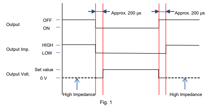
The reverse current means a discharging current for the inductive load. If the discharging current may affect your load state, set Surge Suppression to off.
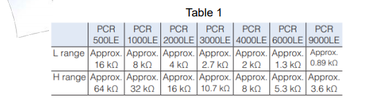
For your reference, Table 1 shows the high impedance value.
1-2. Voltage Waveforms
The following figures are the actual voltage waveforms when the output was turned off with different loads. Conditions: Output 50 Vdc by PCR500LE and turn it off.
No-load state: See Figure 2. The voltage kept at 0 V for approx. 200 microseconds. The undershooting was seen soon after the output shifted to the high-impedance state.
With the lower load resistance (See Figure 3 and 4) or large capacitor (See Figure 5), the undershooting was reduced or almost eliminated.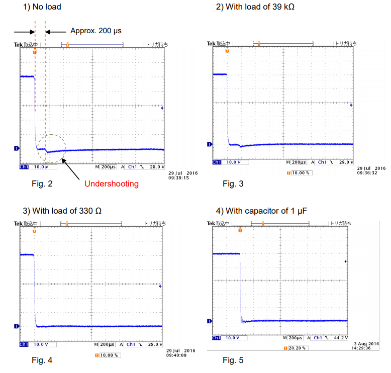
The undershooting was caused by 1) a switching circuit in PCR500LE that switches from low to high impedance 2) capacitors (X-capacitor and Y-capacitor) at PCR500LE’s output terminal and 3) internal wirings in PCR500LE.
Quite small energy was stored into the internal wirings in PCR500LE when the output was turned off. This residual energy was dissipated in the load resistance or capacitance. Thus, the voltage undershooting was suppressed, as shown in Figures 3 through 5.
2. Surge Suppression: Off
You can set Surge Suppression to off;
If you do not want to let the reverse current flow back to PCR-LE/LE2 when the output is turned off, or
If you simulate the event like; While PCR-LE/LE2 provides a DC output to an inductive load, its load cable is suddenly disconnected.
For the instruction how to set Surge Suppression to off, see Appendix in Section 4.2-1. Timing Chart
The timing chart in Figure 6 shows that;
1. The output is in the high impedance state while the output is turned off.
2. When the output is turned on, the output shits to the low impedance state and the voltage rises to the set value.
3. When turning off the output, the output shifts to the high impedance state.
With Surge Suppression turned off, the followings may happen;
The rising voltage becomes unstable.
The voltage overshooting is seen on the rising voltage.
The rising voltage is fluctuated by the load state.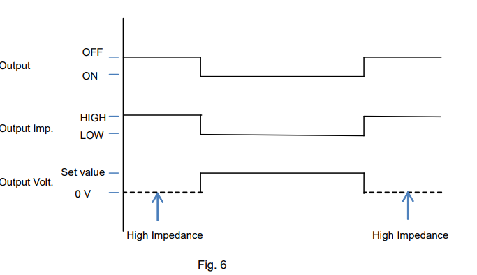
2-2. Voltage Waveforms
See the figures below for the measurement voltage waveforms when the output was turned on and off under the following conditions; Output 50 Vdc by PCR500LE and turn it off in no-load state.
In Figure 7, the rising voltage was somewhat unstable.
In Figure 8, when the output was turned off, the residual energy in PCR500LE was gradually released with high impedance, and accordingly the voltage fell down slowly.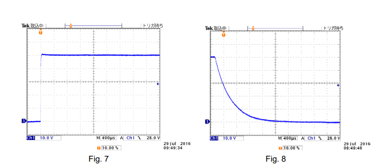
3. Recommendations
Surge Suppression is necessary and useful function; however it cannot provide its optimum performance with the wrong setting. We recommend that you choose whether to turn Surge Suppression on or off depending on the characteristics of your DUT.
Surge Suppression is available with the firmware Ver. 4.50 or later.
If you installed the firmware Ver. 4.50 or earlier, the output on/off operation is fixed as Surge Suppression is set to on, that is, you cannot turn Surge Suppression off.
To update your firmware, visit the following website:
https://www.kikusui.co.jp/en/download/en/?fn=pcr-le_FW
* Also please read the supplementary paper of ‘Voltage Interruption Waveforms Provided by PCR-LE Series’.Necessity of Grounding Output Terminal for DC/AC Power Supply
Power supply has the following three output terminals:
– DC power supply: Positive/negative terminals and Ground (GND) terminal – AC power supply: L/N terminals and GND terminal.
Upon using both power supplies, it is necessary to determine whether either of positive or negative terminals or L/N terminals is connected to the GND terminal.
As our factory default;
– DC power supply: Depending on the series or models, the GND terminal is connected to the negative terminal or floating (non-grounding).
– AC power supply: The GND terminal is floating.
The following information may help you to ground the power supply properly.1. Isolation Block Diagram for Each Terminal
Figure 1 shows how the output (secondary) terminals of AC power supply are isolated from the input (primary) terminals and the GND terminal. The isolation block terminal for DC power supply can be compatible to Fig. 1.
Figure 1 provides the example as: single-phase three-wire, AC200V.
1) The GND terminal at the output side is connected to the GND terminal at the input side. The GND terminal at the input side is required to be grounded by connecting to the ground terminal at the distribution board for safety reasons. If not, please make sure to check the condition of EUT.
2) The output terminals except for the GND terminal are isolated from the input terminals. Isolation is specified in specifications. E.g.) Withstand voltage between the primary and secondary side is AC1500V/1 mins.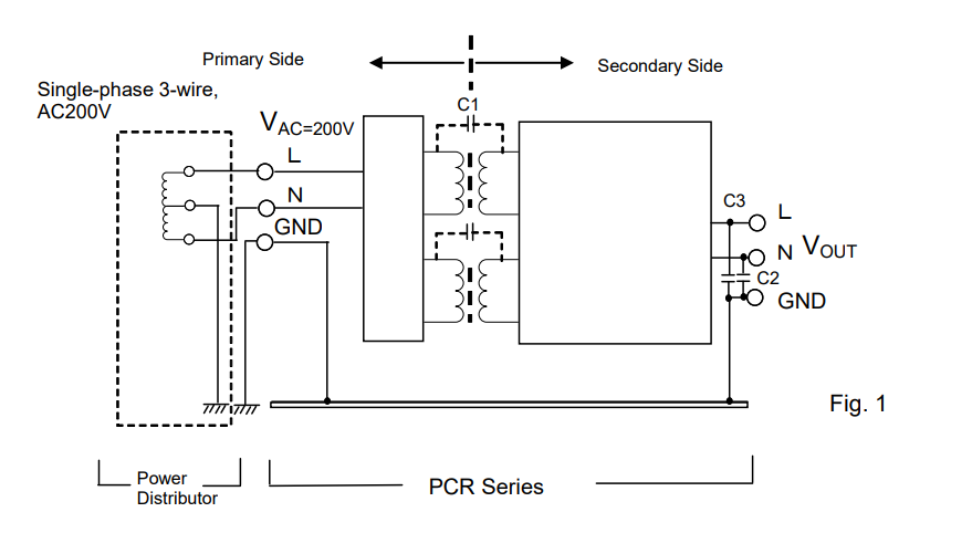
2. Requirement and Effect on Grounding Output Terminal
The requirement and effect on grounding are described in each subsection with case studies.
2-1 Electric Shock Caused by Isolated Power Supply
The following inquiry might be asked: ‘Why did I have an electric shock when I touched the N terminal even the AC power supply is isolated?’
As shown in Figure 1 above, the primary and secondary terminals of power supply are isolated. However, Figure 2 shows that the voltage is divided at the capacitance of C1/C2 and applied to the N terminal. In this case, you may have an electric shock when touching the N terminal.
To avoid this issue, please connect the N terminal to the GND terminal or connect a high-capacity capacitor between the N terminal and the GND terminal.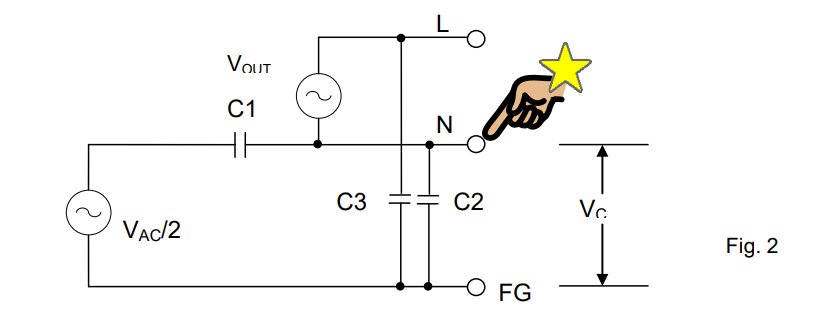
2-2 Power Supply for Swimming Pool Water Treatment
Figure 3 shows the equivalent circuit of the swimming pool water purification system. As you can see, the output from the DC power supply is in the swimming pool. If the isolation between the primary and secondary terminals is not fully secured due to any trouble, the voltage from the primary terminals will be applied into the water. Then, it induces the leakage current into the swimming pool and it may cause an electric shock.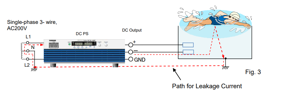
To avoid this issue, please always connect either of positive or negative output terminals to the GND terminal. For the case of 2-1 and 2-2, the grounding is required at the secondary terminals for safety.
2-3 Power Supply for Wireless Transmitter (Ground Connection at High-Frequency)
Figure 4 shows the system that measures the wireless transmitter power. Common-mode noise is generated inside the power supply. In this figure, the output terminals of power supply are connected to the wireless transmitter. Common-mode noise is emitted to the surroundings as shown by the arrow. When the common-mode noise passes through the ground loop, it turns to the current noise (I-noise). Then, when this current noise passes through the cable outer coating, VI will be generated and measured by the spectrum analyser.
To avoid this issue, the output terminal of power supply is connected to the GND terminal to eliminate the common-mode noise.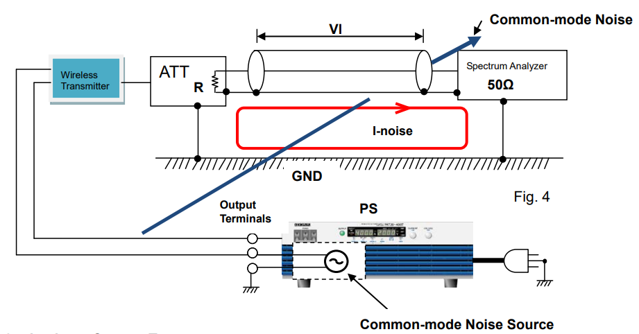
2-4 Leakage Current Test
Figure 5 is referred to the IEC60990 that defines the measurement of leakage current (protective conductor current and touch current). This circuit is equivalent to the measuring of the leakage current when the AC power supply is connected to EUT. In this case, the N terminal should be connected to PE (Protective Earthing = GND terminal) to create the path for leakage current as shown by the red dotted lines.
Since either of output terminals should be grounded to measure the leakage current, AC power supply is suitable for such measurement.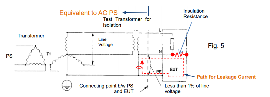
3. Consideration for Voltage to Ground
Voltage to ground is specified for output terminals by product series/models. It means the maximum voltage to be applied between the output terminals (positive/negative or L/N) and GND terminal (chassis potential). In Figure 6, neither V (N-G) nor V (L-G) can exceed the voltage to ground.
For the figures below, if you use the DC power supply, please regard L terminal as positive terminal and N terminal as negative terminal.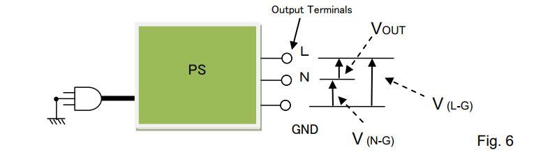
Please be noted that the output voltage applied to the output terminals and GND terminal might be limited depending on the power supply specification.
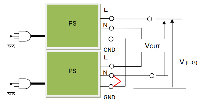
Two examples are listed below with the condition as: Using DC power supply with Rated output voltage= DC300V and Voltage to ground=±DC500V.
Example 1: If DC250V is applied between N and GND, the output voltage (VOUT) is limited to DC250V.
VOUT = Voltage to ground – V (N-G) = 500V – 250V = 250V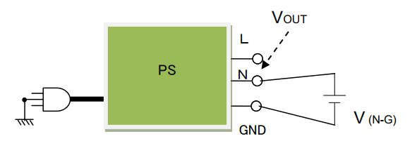
Example 2: Two DC power supplies are connected in series and the N terminal and GND terminal at the second power supply are connected. V (L-G) is DC500V so that the VOUT is limited to DC500V even with two power supplies used.
How to Minimise Power Supply Noise in Test Systems
Noise is an unwanted but inevitable problem in test systems including power supply sources, except batteries, which are low-noise power sources. Some amount of noise is always generated or relayed by power supplies; however, a power supply is a device that supplies power to another device, and not intended to be used by itself. Power supply noise should be low enough so as not to interfere with the neighbouring equipment or test results.
This white paper will discuss how to mitigate the power supply noise in the test systems, showing two test system examples – a DC/DC converter test system and an RF amplifier test system. It particularly explains how to setup the power supply or measurement equipment in the test system, including the wiring method.1. Power Supply Noise in DC/DC Converter Test Systems
Figure 1 shows the test system. The DUT is a DC/DC converter powered by a power supply with a load resistor connected. An oscilloscope measures the output voltage ripple of the DC/DC converter; voltmeter 1 measures the output voltage; the output current can be taken by measuring the voltage across the shunt resistor from voltmeter 2. The input source of the power supply, oscilloscope, voltmeter 1 and 2 are grounded to the GND for safety.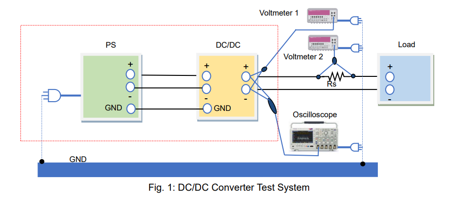
1-1. What is Power Supply Noise?
Power supply noise can be divided into two types: “common mode noise” generated in a ground loop and “differential (normal) mode noise” appearing in the positive and negative lines. The common mode noise is applied on the ground (GND) line and negative line. The GND terminal is grounded when the power cable is plugged into an outlet.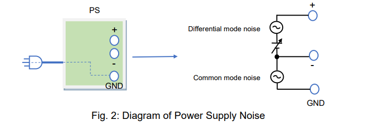
1-2. How to Minimise Power Supply Noise
This section explains how differential mode noise and common mode noise enter a system and how these noises can be reduced.
1) How Differential (Normal) Mode Noise Enters DUTs
The positive and negative cable wiring deliver the differential mode noise to your DUT. How the DUTs reject the noise depends on their power supply rejection ratios (PSRR). The DUT’s tolerance against the differential mode noise can be measured by determining how the noise frequency characteristics affect the outputs of DUTs. For reducing noise, using cable inductance and placing a capacitor with good high-frequency characteristics at the input of your DUT may help. With a wire loop, magnetic flux may be generated due to the differential mode current as shown in figure 3. This noise is emitted into the air, affecting the neighbouring equipment. To suppress this noise emission, twist the positive and negative cables.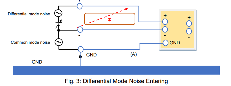
2) How Common Mode Noise Enters DUTs
Common mode noise appears in the positive and negative lines of the power supply carried through the GND contact (common ground). That is to say, common mode noise enters both the GND and negative line. The same amount of common mode noise (voltage) also appears in the positive line, where the differential mode noise (voltage) and DC voltage are applied.
When the common mode noise enters the DUT, it may be converted to the differential mode noise depending on the stray capacitance between the signal line and GND line of the DUT, and this can affect the output performance of the DUT. If there is a large ground loop and wire loop, a magnetic flux may be generated due to the noise current as shown in figure 4, and this noise is emitted into the air, affecting the neighbouring equipment (e.g. measuring devices). To reduce this noise, make the loop smaller. It can be done by grounding the DUT’s GND by following method ‘B’ in figure 5.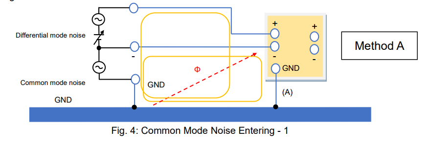
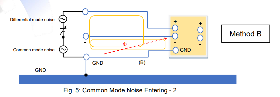
3) Good Defense for Common Mode Noise
In both cases shown in figure 4 and 5 (method ‘A’ and ‘B’), the ground loop is present, so common mode noise and magnetic flux are unavoidable. To prevent common mode noise emission, add a capacitor or short wire between the GND and negative terminals of the power supply as shown in figure 6.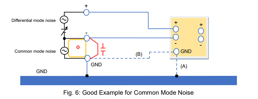
4) Poor Defense for Common Mode Noise
Figure 7 shows an example similar to figure 6: a capacitor or short wire is added between the GND and negative terminals at the input of the DUT. It appears good, but noise currents Iw1 and Iw2 increase, and the magnetic flux becomes stronger than those of figure 4 and figure 5. This causes an electric wave, which can interfere with measuring systems and other neighbouring equipment. It also assists the generation of the differential mode noise (Vw1 – Vw2) due to the difference of the wire impedance.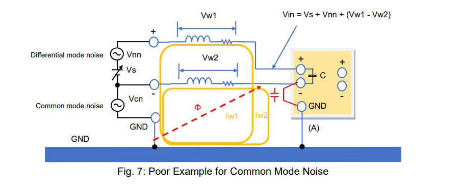
5) Common Mode Choke Coil
In the case of figure 7, if the noise current reduces, the magnetic flux noise can also decrease. In figure 8, after adding a common mode choke coil, the cable impedance on the wire loop will increase. Accordingly, Iw1 and Iw2 will reduce. The common mode choke coil can also block external noise (magnetic flux) so that it can be added in the system example shown in figure 6. Figure 9 shows the relationship between the impedance of the common mode choke coil (Z) and Iw. If Z increases, Iw decreases. As a result, the magnetic flux will decrease.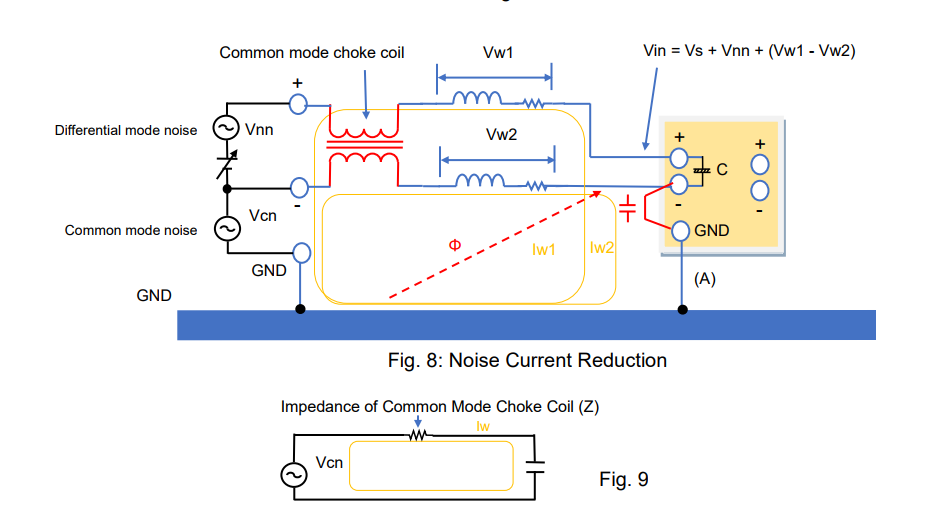
6) Power Supply Noise-Reduction Technique
Now, let’s summarise how to control the power supply noise. Figure 10 shows one example of a reduced-noise test system. If the noise persists on your test system, try the following:
A) Twist the output cables of the power supply. *1
B) Connect the output terminal of the power supply to the GND or connect them with a capacitor.
C) Avoid the ground loop.
*1: It is also effective to apply a common mode choke coil to the power supply output.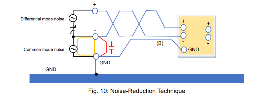
1-3. Power Supply Noise in Measurement Equipment
Figure 11 shows the noise-controlled test system. The DUT is a DC/DC converter. However, even with such system, the power supply noise cannot be fully suppressed. Furthermore, the DC/DC converter inevitably generates noise as well. The DC/DC converter noise can be also classified as differential mode noise and common mode noise.
The test instruments have notable characteristics. The voltmeters are isolated from the power supply’s GND, but the oscilloscope’s GND is connected to it.
This section explains how the common mode noise affects oscilloscope measurements and how to handle it.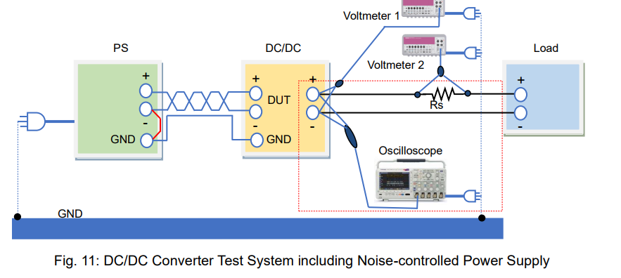
1) How Common Mode Noise Affects Oscilloscope Measurements
Figure 12 shows that the DC/DC converter is measured with the oscilloscope at its input terminal. In the ground loop, the common mode noise voltage (Vcn) appears, and the noise current (Iw2) circulates through the outer conductor of the probe cable. Then noise voltage (Vw2) is generated between the negative terminal of the DC/DC converter and the oscilloscope’s GND. Consequently, the voltage measurement is calculated as Vs + Vnn + Vw2. It is affected by the common mode noise.
The input impedance of the oscilloscope probe is 10 MΩ as shown below, so Iw1 caused by Vcn cannot flow through the center conductor of the probe cable. Accordingly, no noise voltage generates due to Iw1. Only Vw2 is included in the measurements.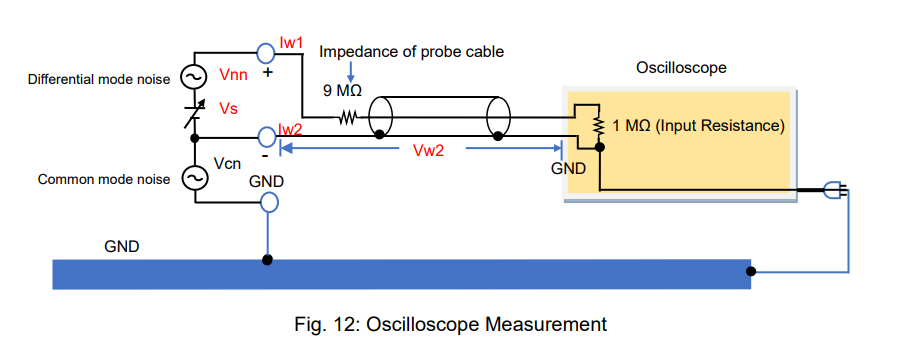
2. Power Supply Noise in RF Amplifier Test Systems
Figure 14 shows a noise-controlled test system. The DUT is an RF amplifier. The RF signal from the RF signal generator is amplified by the RF amplifier. The output of the RF amplifier is measured by a spectrum analyser. RF amplifiers are small signal-tuned amplifiers that amplify small signals at radio frequencies. The chassis of RF amplifiers is at GND potential. Therefore, an external magnetic flux caused by the common mode noise should be removed from RF amplifier measurements.
The magnetic flux can be generated around the output of the power supply as well as from the chassis or power supply line.
This section explains how the external magnetic flux affects the RF amplifier measurements and how to handle the noise.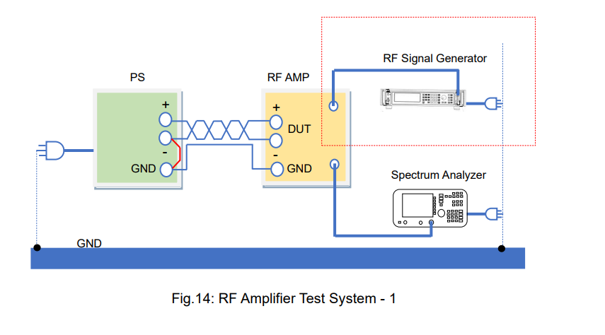
1) Why External Magnetic Flux Affects RF Signals
Figure 15 shows that the RF signal generator output connector is connected to the RF amplifier input port by a coaxial cable. In this system, the ground loop is obviously formed, so if an external magnetic flux caused by common mode noise passes through this loop, the noise current (Iw) flows through the outer conductor of the coaxial cable. Thus, this generates the noise voltage (Vw). Vw is added to the RFSG output through the input port of the RF amplifier. The RF coaxial cable has an impedance of 100 Ω in total at its center conductor. As an external magnetic flux passes this loop, the current does not flow through the center conductor with high impedance, so that the noise current (Iw) only flows through the outer conductor of the coaxial cable. These unbalanced currents lead to adding Vw to the RF signals.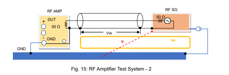
2) How to Minimise Common Mode Noise
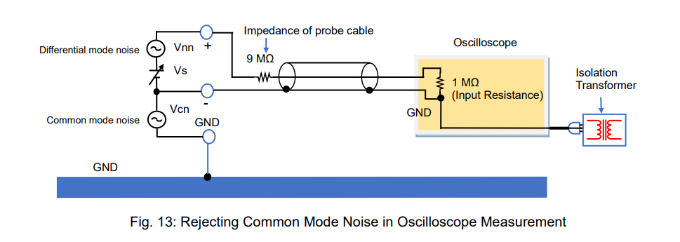
The above noise issue is caused by the ground loop. To solve it, break the ground loop by placing an isolation transformer as shown in figure 16 (see also Sec. 1-3-2 above).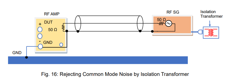
Another solution is to wind the coaxial cable on a toroidal core, which blocks the current from flowing through the outer conductor of the coaxial cable.
Products Mentioned In This Article:
Full range of Kikusui products please see HERE
DC Electronic Load – Part 2: Basic Operation Mode and Principle (1)
As described in Part 1, electronic loads can act as a variable resistor and regulate a current depending on your applications. With this function, electronic loads can be used as substitute for high-power components. To fulfill this function and test DUTs effectively, there are four operation modes for electronic loads: 1) constant current 2) constant resistance 3) constant voltage and 4) constant power. Part 2 and Part 3 will describe each of these modes and the sequence function to simulate the specific electric and electronic components.
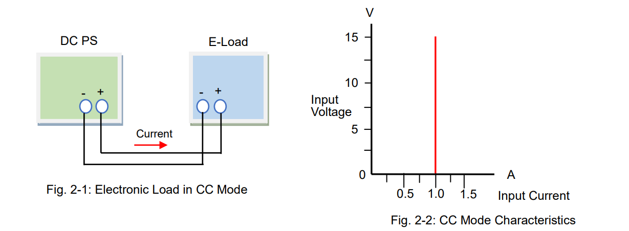
2-1. Constant Current (CC) Mode
In CC mode, an electronic load consumes constant current in regardless of input voltage variations. Figure 2-1 shows the connection diagram between the DC power supply and electronic load. Figure 2-2 shows the input current – input voltage characteristics in CC mode. You can see that the current is constant all throughout despite changes in voltage.
For example, if your test power supply has the output voltage variable range of 10 V ± 1 V, and its rated output current is 1 A, you need to determine whether it can provide 1 A with its output voltage change from 9 to 11 V. So you should prepare an electronic load that constantly consumes the current of 1 A regardless of the input voltage changes from 9 to 11 V.
Figure 2-3 shows the connection diagram. Figure 2-4 shows that the electronic load operates the CC mode regardless of the input voltage changes from 9 to 11 V.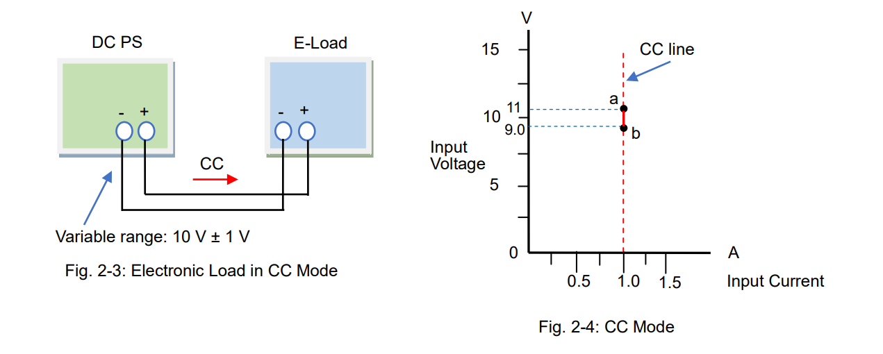
You can also let the electronic load behave as a variable resistor (see also Part 1, Sec. 1-2-1: “Act as Variable Resistor”) but you will need to change the resistance value of the electronic load each time the input voltage changes. This is not efficient because you need to set the resistance and monitor the current all the time. Figure 2-6 shows that the electronic load consumes the current of 1 A by varying the resistance value.
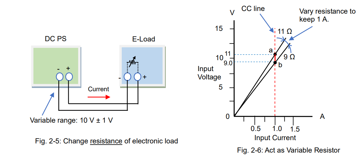
Compared to this method, the CC mode allows you to easily vary the current to flow. The CC operation is intuitive and used for diverse applications.
By the way, what is an operating principle of the CC mode? As stated in Part 1, electronic loads can provide various operations depending on the circuit functions. In CC mode, electronic loads will automatically adjust the resistance value, just like the way of Figure 2-6, to maintain the constant current. In more detail, electronic loads will monitor the current; when the voltage rises, it increases the resistance with reducing the current flow, and vice versa, when the voltage falls, it decreases the resistance to prevent the current from falling.
Operating Principle
Figure 2-7 shows the operating principle diagram of the CC mode. The error amplifier internally controls the current regulator (equivalent to the resistance value) that compares the set current (I) and actual input current detected by the current detector to make them equal. So, the electronic load can constantly absorb the set current (I) by using the feedback control, which is quite popular method in power supplies.
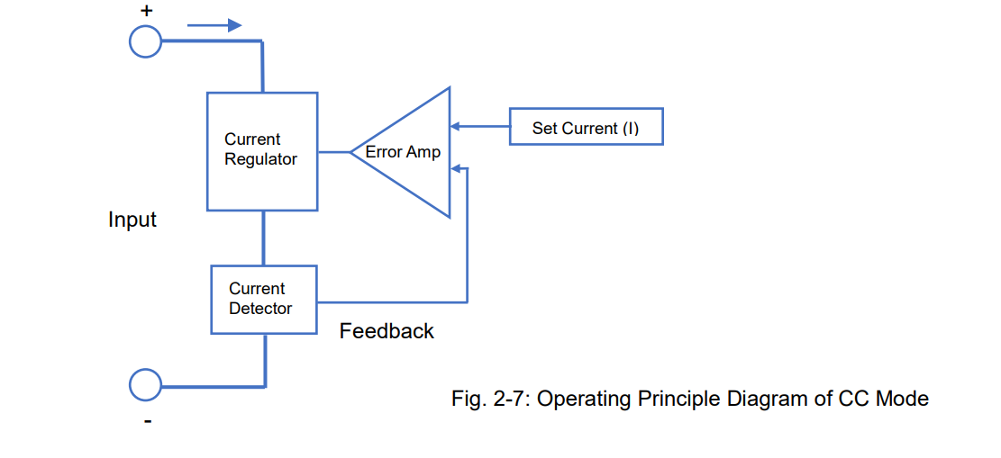
The current regulator in Figure 2-7 controls the current flow. The electronic load circuits have elements such as a transistor or FET rather than a resistance element (see figure 2-6), because they are more electronically easy to control. Figure 2-8 shows the circuit diagram example of the CC mode. In the circuit, the operational amplifier controls the power transistor to make the voltage across the current sense resistor equal to the voltage reference for current setting, so that this circuit enables the CC mode.
The voltage is applied to the electronic load to sink the current. This applied energy is transformed into a heat by the power transistor or power FET so the electronic loads often have a cooling fan.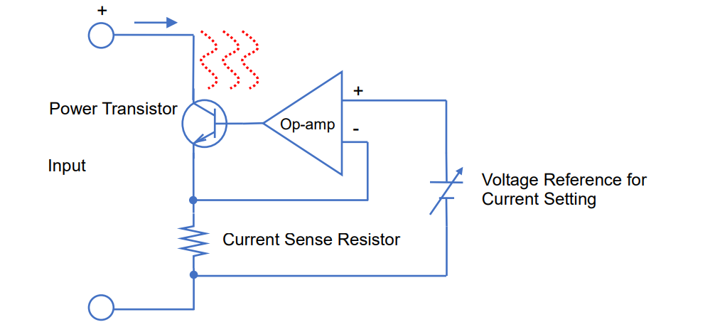
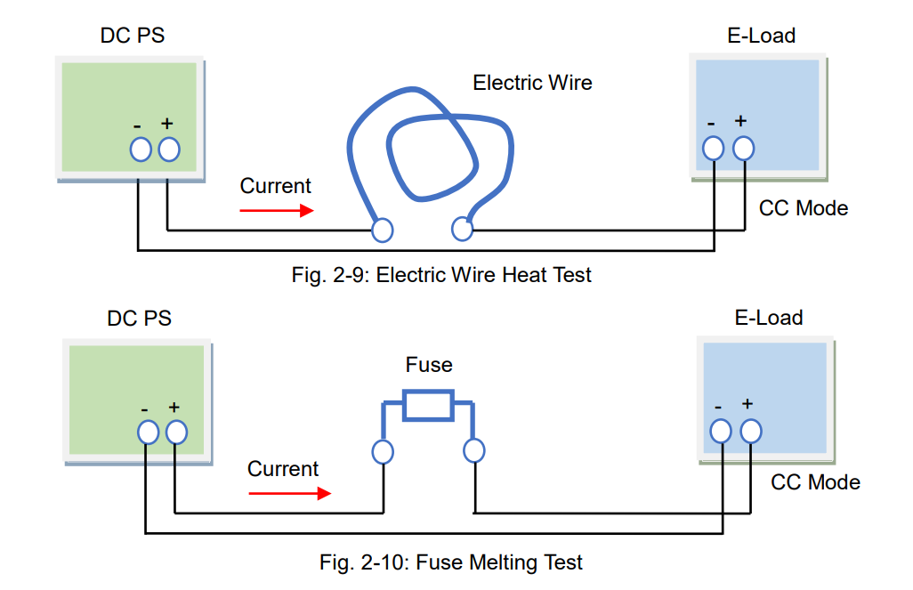
Example Applications for CC Mode – Electric Wire Heat Test and Fuse Melting Test
As a part of the power supply testing, a load regulation test and line regulation test will be performed by the CC mode of electronic loads. During these tests, the output voltage from the power supply will vary within its maximum ratings so the CC mode is suitable for these tests. The other example applications for the line regulation test (CV test) are an electric wire heat test (fig. 2-9) and a fuse melting test (fig. 2-10). The wire resistance and fuse resistance will change significantly when the current flows through them. To sink a constant current from the test samples, use the CC mode of electronic loads.
2-2. Constant Resistance (CR) Mode
The CR mode is a mode that electronic load act as a base component, variable resistor (see also Part 1, Sec. 1-2-1: “Act as Variable Resistor”). When an electronic load has a resistance characteristic like figure 2-11 and 2-12, it operates in CR mode. As shown in figure 2-12, you can adjust the resistance value such as 1 Ω or 3 Ω during the CR mode.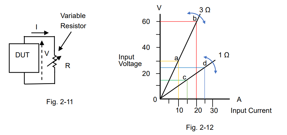
The CR mode is suitable for various applications. It is useful that electronic loads act as a large-capacity variable resistor. One of the typical applications is to test the current limiting characteristic of DC power supplies.
Figure 2-13 shows the connection diagram between the DC power supply and electronic load. The blue straight line in figure 2-14 shows the range that the power supply operates in CV mode. Point ‘a’ shows that the input voltage of electronic load is 50 V with the resistance of 3 Ω. The input voltage moves along this blue line in according with the resistance variations. If the resistance decreases and the input voltage will reach point ‘b’, then the voltage moves along the red line. When the resistance turns to 1 Ω, the input voltage will reach point ‘c’. While the input current is on the red line, the output current from power supply is regulated by 25 A.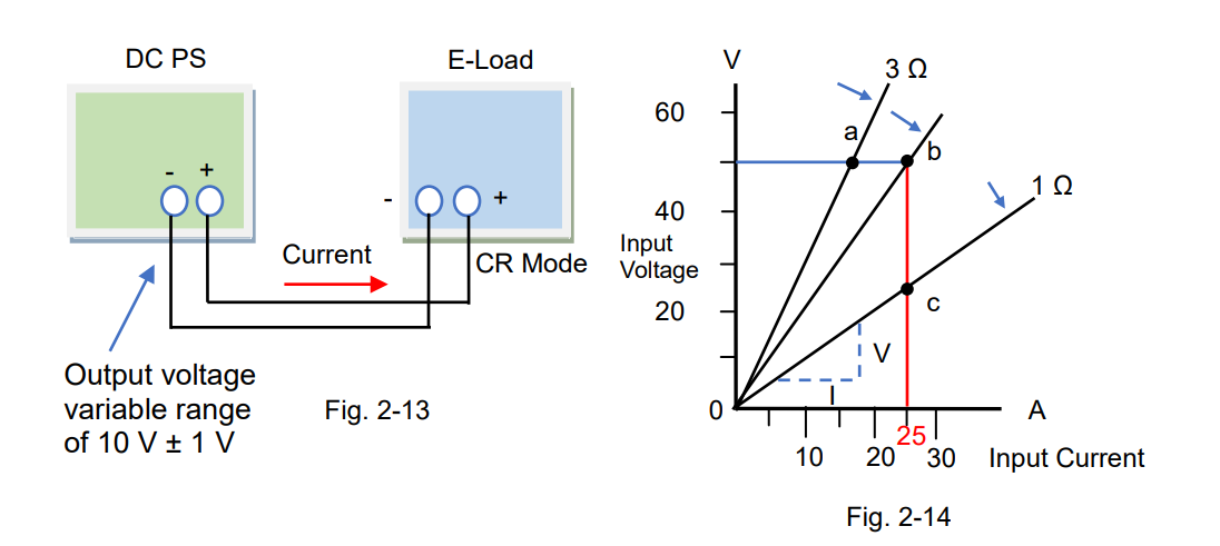
The CR mode is also constructed in the circuit functions of electronic loads. The resistance (R) is calculated by R = V/I. In figure 2-14, the resistance is the slopes.
Operating Principle
Figure 2-15 shows the operating principle diagram of the CR mode. The left side of the diagram is the same as shown in figure 2-7 and the right side shows the component to be used for the CR mode. The multiplier will multiply the input voltage (V) by the reciprocal of set reference (1/R), so the multiplier will output V/R. It equals to ‘V/R = I’, so when V is applied the current will flow according to ‘I = V/R’. That is, the set reference R (= V/I) is constant and this circuit operates in CR mode based on R. The figure below uses the reciprocal of set resistance (1/R), so you adjust it by R. 1/R is conductance G (in Siemens S).
For the current regulator, a power transistor or power FET are usually used.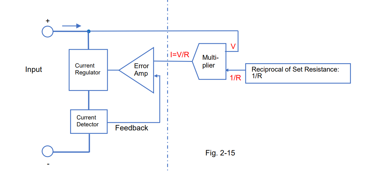
Example Applications for CR Mode – Switch Life Test
The example application for the CR mode is the switch life test. Figure 2-16 shows the test system that the switch is placed between the DC power supply and electronic load to repeat the on-off switching tests. Excellent test-reproducibility can be achieved from this system because the CR operation avoids the rapid current on-off switching.
(Note: The current rise time differs depending on the electronic load performance.)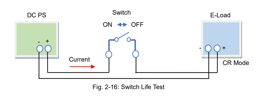
Products Mentioned In This Article:
- Kikusui Electronic Loads please see HERE
What Makes a Good Power Supply?
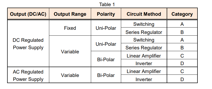
DC or AC regulated power supplies (hereinafter called ‘power supply’) can be classified into eight types and four categories in accordance with the output source (DC or AC), output range, polarity or circuit method as shown in Table 1.
In this white paper, we look at four characteristics associated with the power supply’s specification: line regulation, load regulation, transient response and ripple noise. We also discuss how to determine the ability of the power supply by these four characteristics. Note: This white paper refers to the constant voltage characteristics based on an AC line input.
1. Line Regulation
Firstly, here’s how electricity gets to your power supply: 1) Power plants generate electricity. 2) Electricity travels via a power grid. 3) Electricity is distributed by a circuit breaker at your home or office. The circuit breaker is connected to each of electrical outlets by wiring. 4) Finally, electricity travels through these wires to the outlets where your power supply is plugged in.
See Figure 1 below: if some electricity consumers on the same distribution line consume large electric power, the utility voltage drops, and vice versa, if they consume less power, the utility voltage rises. A good power supply can keep its output voltage stable despite the utility AC voltage fluctuation.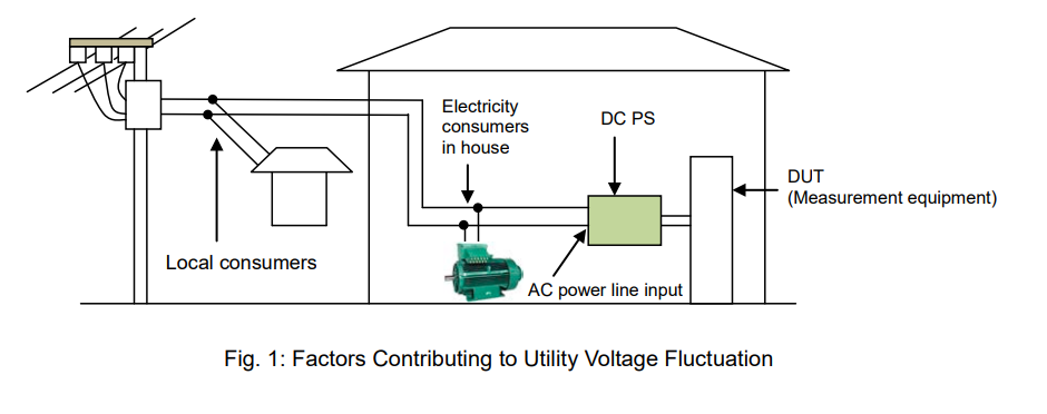
Line regulation is changed in power supply output voltage due to variation of input line voltage. It is expressed as an actual change value in the output voltage relative to the ±10% change in the input line voltage (The standard input line voltage is: 120 Vac in U.S.A and 100 Vac in Japan). For industrial power supplies, the change in the input line voltage may be defined as ±15%. The input voltage at which the power supply is designed to work (such as the standard voltage ±10% or ±15% as above) is the rated input voltage.
The performance specification for the power supply is ensured within the rated input voltage. Some power supplies define a wide rated input voltage range under the specific line regulation. In general, a good power supply has small line regulation but it is difficult to develop.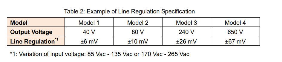
*1: Variation of input voltage: 85 Vac – 135 Vac or 170 Vac – 265 Vac
2. Load Regulation
A load on an electrical system is any device, part or portion of a circuit to which power is drawn from a power supply. So, how do you find which power supply can deliver enough current to your load? To choose an appropriate power supply to your load, check the rated output current, maximum load current that a power supply can provide, specified on its product data sheet. Furthermore, in fact the load current is affected by the load variation.
If the output voltage of your power supply significantly changes with the load variation: ● Your load may be damaged due to an unstable output voltage.
● Test data reliability or test reproducibility cannot be ensured due to the test voltage variation. Load regulation measures how much the output voltage is affected by the load variation from 0 to 100% (no load to full load).
A good power supply has small load regulation.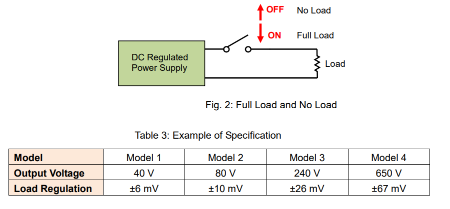
3. Transient Response
For example, the load regulation can be measured by the formula:
‘output voltage value after keeping a no-load state for 10 seconds’ – ‘output voltage value after keeping a full-load state for 10 seconds’.
This formula indicates that: ‘No-load voltage under a stable output voltage’ – ‘Full-load voltage’. The output voltage dynamically fluctuates while in the load current variation such as when a load is switched from no-load state to full-load state and vice versa. Transient response is the response characteristic how a power supply responds to a sudden load variation, that is, the time until an output voltage reaches a steady-state.
Note: Some power supplies define a no-load voltage as 10-plus % of a full-load voltage.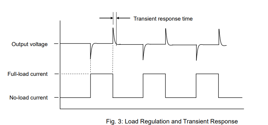
It is important how fast a power supply returns back to a steady-state. In other words, a good power supply has an excellent transient response time.
A power supply should provide a faster enough transient response to a load, otherwise a load current fluctuates before an output voltage returns to a steady-state and an output voltage becomes unstable.
See Table 4 for the reference value of the transient response time for each category of power supply.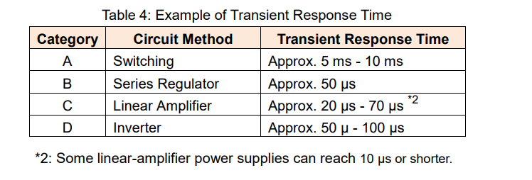
4. Ripple Noise
A power supply consists of several components such as a power electronics circuit that converts a utility AC to a stable DC/AC output. To provide a stable voltage output, a power supply performs a negative feedback control; however ripple noise can be prevalent during this negative feedback operation. Figure 4 shows the typical waveform for ripple & noise generated from a power supply.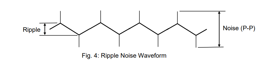
If your power supply generates a ripple noise, it will be superimposed on your DUT’s output voltage.
Especially with a high ripple noise, the following malfunctions may occur to your DUT:
A) If your DUT has a digital circuit:
● An input voltage for your DUT exceeds its threshold level and it may cause a malfunction on the digital circuit of your DUT.
B) If your DUT has an analogue circuit:
● Ripple noise is superimposed on your DUT’s output and it may reduce the quality of your DUT’s analogue signal.
Ideally, a good power supply has little ripple. In practice, however, you will purchase a power supply within a reasonably low-price range unless above malfunctions have been discovered. So, you may need to reduce the ripple noise depending on your power supply in use. If you want to know how to reduce the ripple noise, read the appendix below.
The higher the rated output voltage, the higher the ripple noise is provided by the power supply. Table 5 shows the typical ripple noise value according to the power supply category. Some power supplies may give the rms value and peak-to-peak (P-P) value of the ripple noise.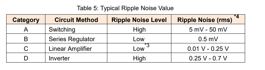
*3: If a linear-amplifier power supply incorporates a switching regulator, a ripple noise may increase. A lower ripple noise may be achieved by high-speed bipolar DC power supply.
*4: Measurement frequency bandwidth: 10 Hz to 1 MHzAppendix: How to Reduce Ripple Noise from Power Supply
1. How to Reduce Ripple Noise
1) Connect negative output terminal of power supply to ground
Connect a negative output terminal and a ground terminal to minimize a high frequency common mode noise generated between both terminals. Figure 1 shows that a capacitor is placed between both terminals. If your DUT is accepted, connect both terminals by a conducting wire.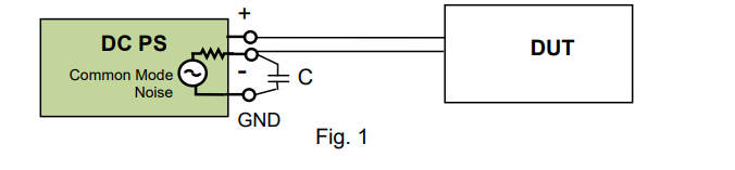
2) Place capacitor at feeding point of DUT
Place a capacitor (approx. 0.1 µF – 1 µF) at a feeding point of your DUT to reduce a high frequency common mode noise. This method is effective when the wiring distance from a power supply to a DUT is long.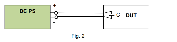
2. Precautions for Ripple Noise Measurement
When an rms value is measured by a true rms meter or a noise is measured by an oscilloscope, place an isolation transformer between the true rms meter or oscilloscope and the power source line as shown in Figure 4. The isolation transformer eliminates a high frequency common mode noise to minimize measurement errors.
As shown by the red line in Figure 3, the common mode noise current is generated from the DC power supply and passes through the ground and returns to the power supply line. If the current flows through the probe cable jacket of the oscilloscope, the voltage Vn is generated and added to the measurement. The isolation transformer can eliminate this voltage Vn.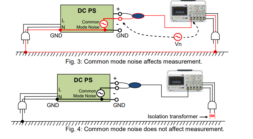
Products Mentioned In This Article:
What It Takes to Keep Regulated DC Power Supply Stable Part 2: Load Conditions
Basically, a regulated DC power supply (referred as DC power supply) is an electrical device that provides a constant output voltage; however, sometimes it cannot remain stable. There might be some factors that affect the stability of the DC power supply, and Part 1 previously focused on one of them: how you connect cables on a system. Here in Part 2, we look at one other important factor that needs to be considered: load conditions. Ensuring that your system runs smoothly may rely on the characteristics or state of your load.
In this white paper, we help you understand the typical issues involved with load conditions and how to solve them, particularly focusing on three types of loads: 1) inductive load 2) capacitive load such as battery and 3) regenerative load one by one.
1. If you use inductive load
An inductive load such as a coil of wire is a passive element designed to store energy. When a current flows through it, electromagnetic energy gets stored. This stored energy is released creating reverse current right after its power source is disconnected. Without any protection, an inductive voltage spike, which is always opposite polarity, is seen across the inductive load when its supply current is suddenly interrupted.
See Figure 1 below. As an inductive kickback protection, usually a diode (‘D1’) or equivalent diode in a low-impedance state is placed in parallel with output terminals of a DC power supply. When the output is turned off, D1 can make a path for an inductive current (‘IL’) to suppress an inductive kickback, and thus D1 can protect the DC power supply.
Meanwhile no big noise occurs. This is because; 1) The output-off speed is slow at a microseconds-order interval. 2) IL through D1 never exceeds the current through the inductance in the load. 3) The current for this system can keep the small variations.
Particularly, D1 is so-called a flyback diode.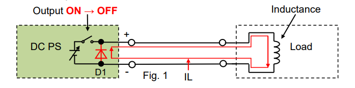
As shown in Figure 2, if another switch is placed to control the DC power supply’s output, there is no longer any path for IL so that a reversed voltage spike is induced when an output is turned off. As for the switching on/off speed, it is quite fast and the fastest one will be 1 µs or less. If a supply current is suddenly interrupted at this speed, an induced voltage across the inductance (‘L’) will become significantly higher as calculating: ‘V = L x dI/dt’.
As you can see below, a stray capacitance creates a loop for this high-frequency high voltage and a load wiring acts like an antenna to generate an EM noise. Once the noise enters into the DC power supply or any other devices in the system, it may deteriorate their performance or cause malfunction.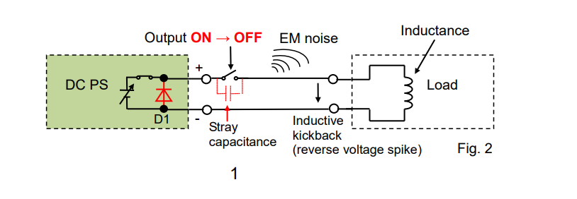
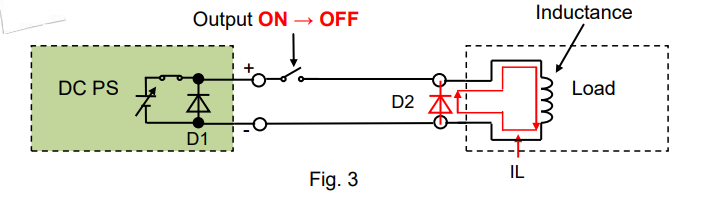
To reduce the noise, place a diode (‘D2’) close to the inductance as shown in Figure 3 to let IL flow through D2.
2. If you use capacitive load such as battery
2-1 Place diode in series
When charging a rechargeable battery, we should take care of a potential difference between a supply voltage and battery voltage. If the supply voltage is lower than the battery voltage, a power source such as a DC power supply acts like its output is turned off, and then the output voltage becomes equal to the battery voltage.
Usually, the DC power supply equips a bleeder circuit (‘R1’ in Figure 4) that let a battery discharging current (‘IBR’) flow through R1. Once IBR flows through RI, the battery will get discharged. Figure 5 shows that IBR is linearly proportional to the battery voltage.
If the output is kept to be turned off or the supply voltage is always lower than the battery voltage, the battery will be fully discharged.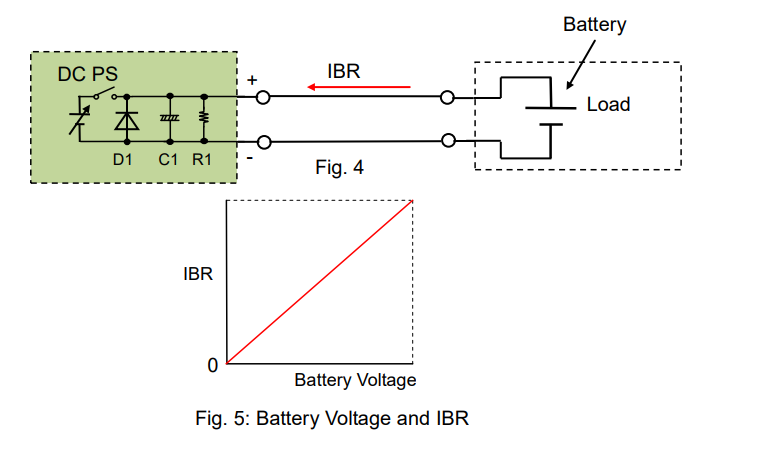
To block IBR, place a diode (‘D2’) in series as shown in Figure 6.
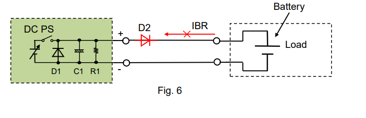
2-2 Remote sensing function
Battery charging is generally done with constant current constant voltage (CC-CV) method. In this mode, a battery is initially charged in CC mode until a battery voltage reaches a certain charging level, and then the charging process is switched to CV mode. This is to ensure that the voltage across the battery terminals does not exceed the maximum rated voltage of the battery while keeping the battery fully charged.
While in CC-CV mode, and a remote sensing function is turned on, you may want to put a remote sensing point at the battery terminals as shown in Figure 7. If so, the output voltage will fluctuate and worse still, the battery may be discharged through the sensing cable. This happens because a non-linear control is given by D2 or a voltage drop may occur with D2 at the battery terminals and it cannot be fully offset by the remote sensing function.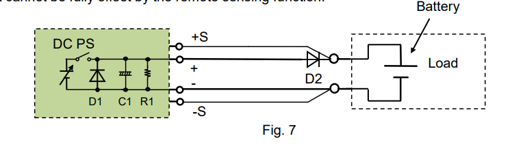
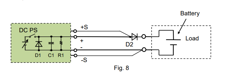
To avoid this, move the sensing point in front of D2 as shown in Figure 8. This can ensure that the DC power supply maintains the stable output. However, you should take care of the voltage drop caused by D2.
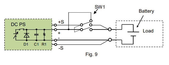
If you do not want D2 but want to use the sensing function, place a switch (SW1) on the sensing wiring (See Figure 9) to simultaneously turn on/off the both switches. In this case, when the DC power supply has the same voltage as the battery, turn SW1 on. To maximize the system efficiency, it is important to minimize the variations from the battery charging current and battery reverse (discharging) current.
3. If you use regenerative load
3-1 Sink current capability by DC power supply
The bleeder circuit (R1) in a DC power supply can absorb a current, typically by several percent of its rated output current*.
If a reverse current (‘IR’) exceeds this level, an output voltage from the DC power supply unintendedly increases, and it may activate an overvoltage protection of the DC power supply. *Bipolar power supply can sink the same amount of the rated output current.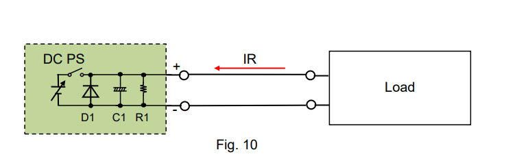
3-2 How to improve sink current capability
For example, let’s look at automotive components such as an electronic power steering (EPS) or a starter generator (SG). Both components use a brushless motor, and when it reverses the motor direction, the energy returns back to the power source. This is the regeneration process. In an actual car operation, the regenerative energy is going back to a car battery.
Let’s return to a DC power supply. While supplying power to such regenerative components, the DC power supply by itself cannot absorb their regenerative reverse current (IR).
See Figure 11 for the countermeasure; An electronic load or a resistor is placed on the load wiring to absorb IR. The electronic load is more efficient because it can easily control a maximum amount of IR.
For this system, it should be noted that the DC power supply should supply IR to the electronic load at least and the load current as needed. Please choose a DC power supply with a large enough current capacity to cover both currents.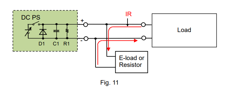
Products Mentioned In This Article:
- DC Power Supplies please see HERE